
Professional PCB manufacturing and assembly
Building 6, Zone 3, Yuekang Road,Bao'an District, Shenzhen, China
+86-13410863085Mon.-Sat.08:00-20:00

Classification of holes on PCB and their functions
1. Classification of vias
In terms of function, vias can be divided into two categories: one is used for electrical connection between layers; the other is used for fixing or positioning components. From the perspective of process, vias are divided into three categories, namely blind holes, buried holes and through holes.
Blind holes are located on the top and bottom surfaces of the circuit board, have a certain depth, and are used to connect the surface layer and the inner layer. The depth of the hole usually does not exceed a certain ratio (aperture).
The buried hole is located in the connection hole of the inner layer of the circuit board, and it does not extend to the surface of the circuit board. The above two types of holes are located in the inner layer of the circuit board, and are completed by through-hole forming process before lamination.
A through hole refers to a hole that passes through the entire circuit board and can be used to realize internal interconnection or as a mounting positioning hole for components. Because the through hole is easier to realize in the process and the cost is lower, it is used in most PCB proofing.
2. The composition of vias
From a design point of view, the via hole is mainly composed of two parts, one is the drill hole in the middle, and the other is the pad area around the drill hole. The size of these two parts determines the size of the via. When designing high-speed, high-density PCBs, designers always hope that the smaller the vias, the better, so that more wiring space can be left on the board. However, the reduction in hole size brings about an increase in cost, and the size of the via hole is limited by drilling and electroplating technology: the smaller the hole, the longer it takes to drill the hole, and the easier it is to deviate from the center; and When the depth of the hole exceeds 6 times the diameter of the drilled hole, it is impossible to ensure that the hole wall can be evenly plated with copper. Three kinds of vias
Most of the situations we usually encounter are pure through-hole PCBs. Boards with blind holes may be due to very high PCB layout density. Some devices with high pin numbers are pasted on the front and back, and blind holes are drilled to solve the high-density problem. Of course, the cost will also increase compared with the cost of through holes. With blind holes, PCBs are generally called HDI PCBs (do you feel familiar, HDI means high density). Buried holes are rarely used. This thing may be like buried capacitance (capacitors are hidden inside the PCB), which is very rare.
A via connects the traces of different layers together as shown in the figure below. The through holes we commonly use are generally mechanical drilling (there are mechanical ones, and there are others, such as laser holes). First press all the layers of the PCB, and after pressing into a PCB, drill through the PCB one by one like nails to form through holes one by one. The inside of the through hole needs to be plated with copper, and there is a relatively large circular metal plate called a pad at the connection of the signal. Of course, when a Via passes through all layers, if there is no connection on a certain layer, then this layer will not have a large hole pad, on the contrary there will be an anti-pad. The anti-pad can be simply understood as a forbidden area that prevents the contact between the via hole and the first layer of metal copper foil. The anti-pad is actually very critical, especially in high-speed and high-frequency PCB design, you often hear the word that engineers hang on their lips is "dig the anti-pad". As for what is anti-pad digging, let’s talk about it later when we talk about SI.
Figure 2 Through-hole 3D
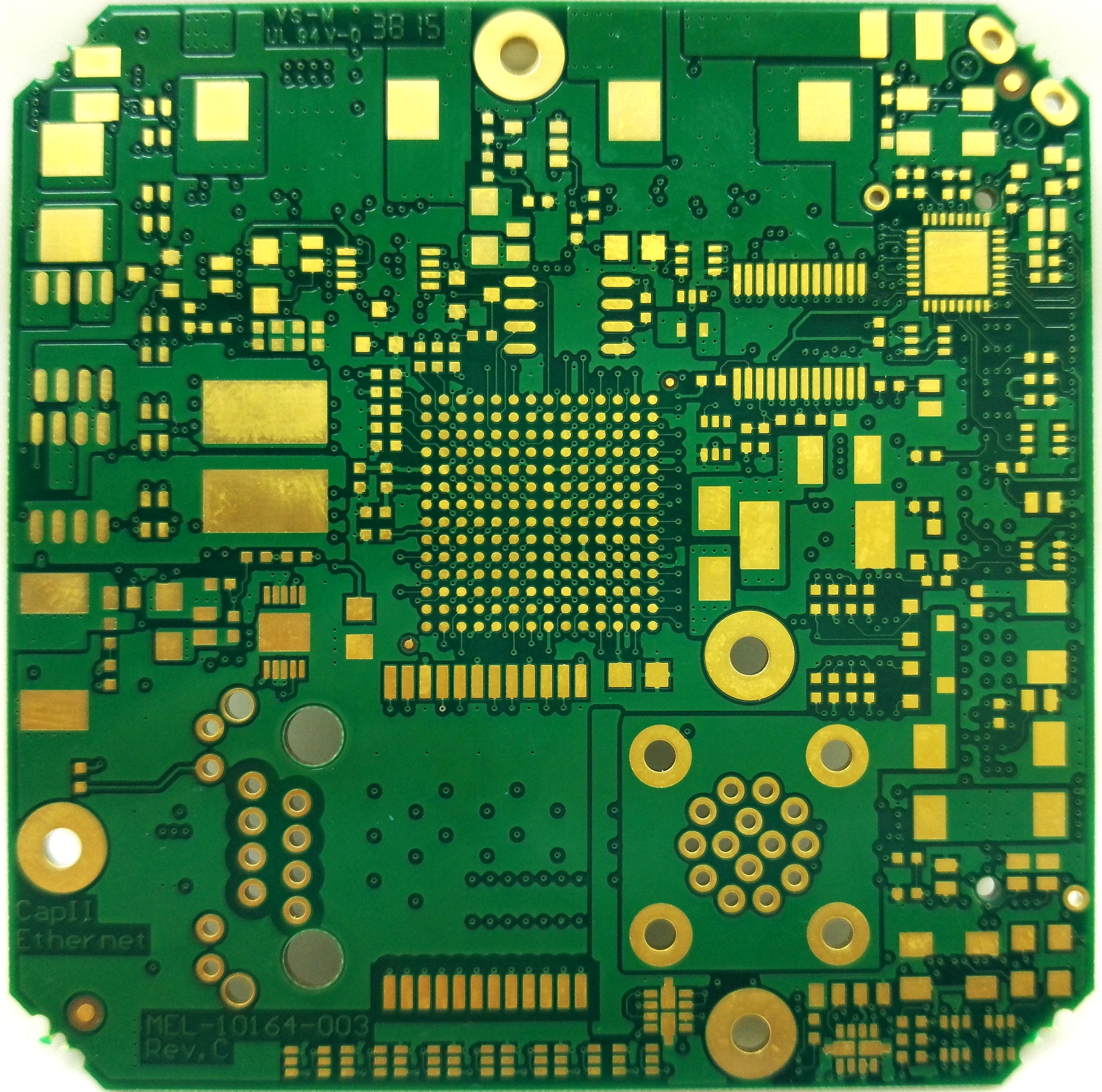
In PCB design, such as large BGA chips and multi-row connectors, a large area is required for FANOUT, and the signal is led to the inner layer through the nearest via hole. The picture below is a BGA chip with thousands of pins. FANOUT always feels beautiful. Based on the size of our chip pins and the PCB thickness-to-aperture ratio (thickness-to-diameter ratio) processing requirements for vias, the vias we commonly use are generally 8mil, 10mil, and 12mil apertures.
The holes on the PCB are divided into plated holes (PTH) and non-plated holes (NPTH) according to whether they participate in electrical connection.
plated through hole
(PTH) refers to a hole whose wall is plated with metal, which can realize the electrical connection between the inner layer, the outer layer, or the conductive patterns on the inner and outer layers of the PCB. Its size is determined by the size of the drilled hole and the thickness of the plated metal layer. Non-plated holes (NPTH) are holes that do not participate in the electrical connection of the PCB, that is, non-metallized holes. According to the level of the holes through the inner and outer layers of the PCB, the holes can be divided into through holes, buried holes and blind holes.
Through-holes run through the entire PCB and can be used to achieve inner-layer connections and/or positioning and installation of components. Among them, the holes used for component terminals (including pins and wires) to be fixed and/or electrically connected to the PCB are called component holes. Plated-through holes that are used for internal layer connections but do not insert component leads or other reinforcement materials are called via holes. There are two main purposes of drilling through holes on the PCB: one is to create an opening through the board, allowing subsequent processes to form electrical connections between the top, bottom, and inner layers of the board; the other is to enable the installation of components on the board. Maintain structural integrity and positional accuracy. [1] Blind and buried vias are widely used in high-density interconnect HDI.
Blind vias typically connect layer 1 to layer 2. In some designs, blind vias can connect layer 1 to layer 3. Combining blind and buried vias enables more connections and higher board density required by HDI. This enables increased layer density in finer-pitch devices, while also increasing transmitted power. Hidden via holes help keep the board light and compact. Blind and buried via designs are common in complex, lightweight, and high-cost electronic products such as mobile phones, tablets, and medical equipment. [2] Blind holes are formed by controlling the drilling depth or laser ablation. The latter is the more common method used today. The stack of vias is formed by sequential lamination. The resulting vias can be stacked or staggered, adding additional steps to manufacturing and testing, as well as cost. According to the use and functional classification of the holes, it is divided into: vias (via) are metallized holes that realize the electrical interconnection between different conductive layers on the PCB, and are not used for plugging in components.
PS: The vias here can be subdivided into through holes, buried holes, and blind holes according to the layers that penetrate the inner and outer layers of the PCB. Component holes are used for soldering and fixing plug-in electronic components and connector holes, usually metallized holes, and can also be used as electrical interconnections between different conductive layers.
Mounting holes
A hole with a larger diameter on the PCB is used to fix the PCB to a carrier such as a housing.
slot
In the drilling program of the drilling rig, it is automatically converted into a collection of multiple single holes or a groove processed by milling, which is generally used as the installation of the pins of the plug-in device, such as the oval pins of the socket.
back drilling
A hole with a certain depth (larger than the previous plated through hole) is drilled on the plated through hole to block the stub of the through hole and reduce the reflection during signal transmission.
The following are some auxiliary holes that PCB board factories will use in the PCB manufacturing process. PCB design engineers can get a general understanding: the positioning holes are three or four holes on the top and bottom of the PCB, and other holes on the board are based on this. Also known as target hole or target hole, it is made by a target hole machine (optical punching machine or X-RAY drilling machine, etc.) before drilling, and is used for pin positioning and fixing when drilling. Inner Layer Alignment Holes There are some holes on the edge of the multilayer board, which are used to judge whether the multilayer board has offset before drilling holes in the board drawing, so as to determine whether the drilling program needs to be adjusted. The code hole is a row of small holes on the bottom side of the board, which is used to indicate some production information, such as product model, processing machine, operator code, etc. Now many factories will replace it with laser typing. The tail holes are some holes of different sizes on the edge of the plate, which are used to identify whether the drill diameter is correct during the use of the drill bit. Now many factories will replace it with other technologies. Slice Holes Plated through holes for PCB slice analysis, which can reflect the quality of the holes. Impedance Test Holes Plated through holes for testing PCB impedance. Fool-proof holes are generally non-plated holes, which are used to prevent the position of the board from being reversed, and are often used in the positioning of molding or imaging processes. Tool holes are generally non-plated holes and are used for related processes. Rivet hole Non-plating hole, used for rivet fixing of each layer core board and bonding sheet when multilayer boards are laminated. When drilling, it is necessary to drill through the position of the rivet to prevent residual air bubbles at this position, resulting in subsequent explosion.
Electronic Components Procurement Summary
May 30,2023


Just upload Gerber files, BOM files and design files, and the KINGFORD team will provide a complete quotation within 24h.