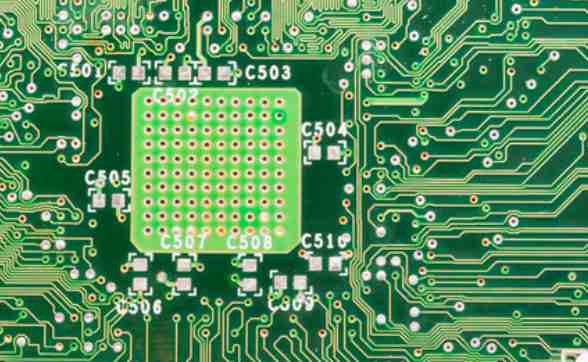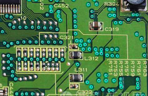
I don't know if you have noticed this phenomenon: most PCB designs have an even number of layers, such as the common four layer board, six layer board. Why is that? In fact, even layer PCBS do have more advantages than odd layer PCBS.
Why are PCB design layers mostly even
Advantages of even layer PCBS
1. Low cost
Due to the lack of a layer of medium and foil, the raw material cost of odd-numbered PCBS is slightly lower than that of even-numbered PCBS. But the processing cost of odd layer PCB is obviously higher than that of even layer PCB. The machining cost of the inner layer is the same, but the foil/core structure significantly increases the machining cost of the outer layer.
Odd - layer PCB needs to add non - standard laminated bonding technology on the basis of the core structure technology. A plant that adds foil to a nuclear structure will be less productive compared to a nuclear structure. The outer core requires additional treatment before laminating, which increases the risk of scratching and etching errors on the outer layer.
Why are PCB design layers mostly even
2. Balance the structure to avoid bending
The best reason for PCB design without odd layers of PCB is that it bends easily. When cooling the PCB after the multilayer circuit bonding process, different laminating tension will cause the PCB to bend as the core structure and the foil-coated structure cool. As the board thickness increases, so does the risk of bending a composite PCB with two different configurations. The key to eliminate circuit board bending is to use balanced layering. Although some degree of bent PCBS meet the specifications, subsequent PCBA processing will be less efficient, resulting in increased costs. Because assembly requires special equipment and processes, it reduces the accuracy of parts placement and thus damages quality.
Change is easier to understand: In the process of PCB technology, four-layer board is better than three-layer board control, mainly in the aspect of symmetry, the warpage degree of four-layer board can be controlled below 0.7% (IPC600 standard), but the size of three-layer board, warpage degree will exceed the standard, which will affect the reliability of SMT and the whole product, so for general PCB designers, do not design odd layer board. Even with the odd layer function, the counterfeit design is even layers, the five-layer PCB design is divided into six layers and the seven-layer PCB design is divided into eight layers.
Based on the above reasons, PCB multilayer design mostly uses even layer, rarely uses odd layer.

Why are PCB design layers mostly even
How to balance cascading and reduce the cost of odd-layer PCBS?
When an odd number of PCB layers are present in a PCB design, the following methods can be used to balance the cascade, reduce the cost of PCB production and avoid PCB bending.
1. Add a signal layer and leverage it
You can use this method if the PCB has even power layers and odd signal layers. Adding layers does not increase costs, but can reduce lead time and improve PCB quality.
2. Add additional power layers
You can use this method if the PCB has an odd power layer and an even signal layer. An easy way to do this is to add a layer in the middle of the stack without changing other Settings. First, arrange an odd number of layers on the PCB, then copy the middle layer and label the remaining layers. This is similar to the electrical properties of foils applied in thickened layers.
3. Add a blank signal layer near the PCB board center
This method minimizes stack unbalance and improves PCB quality. First the odd-numbered layers of wiring are added, then the blank signal layer is added, marking the remaining layers. It is used in microwave circuits and mixed media (dielectric constant is different) circuits.
Characteristics of PCB board microhole mechanical drilling
In the rapid update of electronic products now, PCB printing from the previous single-layer board expanded to double-layer board and high precision requirements of more complex multi-layer board. Therefore, the circuit board hole processing requirements are more and more, such as: the aperture is smaller and smaller, hole and hole spacing is smaller and smaller. It is understood that epoxy resin matrix composites are used more in plate factories now. The definition of hole size is that the diameter below 0.6mm is small hole, and the diameter below 0.3mm is micro hole. Today I will introduce the processing method of small holes: mechanical drilling.
In order to ensure high processing efficiency and hole quality, we reduce the ratio of defective products. During mechanical drilling, both axial force and cutting torque are taken into account which may directly or indirectly affect the quality of the hole. Axial force and torque with the feed, the thickness of the cutting layer will also increase, then the cutting speed will increase, so that the number of cutting fibers per unit time will increase, the amount of tool wear will increase rapidly. Therefore, different sizes of holes, drill tool life is not the same, operators should be familiar with the performance of the equipment in time to replace the drill tool. This is why the cost of processing small holes is higher.
In the axial force, the static component of FS affects the wide cutting of the transverse edge, while the dynamic component of FD mainly affects the cutting of the main cutting edge. The dynamic component of FD has a greater effect on the surface roughness than the static component of FS. Generally, when the aperture of prefabricated hole is less than 0.4mm, the static component FS decreases sharply with the increase of the aperture, while the dynamic component FD decreases flatly.
The wear of PCB bit is related to cutting speed, feed rate and slot size. The ratio of bit radius to glass fiber width has a great influence on tool life. The larger the ratio is, the larger the cutting fiber bundle width is, and the higher the tool wear is. In practice, the 0.3mm drill tool life can drill 3000 holes. The bigger the drill knife, the fewer holes will be drilled.
In order to prevent drilling when encountering stratification, hole wall damage, stains, burrs, these problems, we can in the stratification of the first in the following put a 2.5mm thickness of the plate, the copper plate on the plate above, and then on the copper plate above the aluminum, aluminum role is 1. Protect the surface of the board will not wipe flowers. 2. Good heat dissipation, the drill will generate heat when drilling. 3. Buffer function/lead function to prevent deviation hole. The way to reduce burrs is to use vibration drilling technology, using carbide drill bit drilling, hardness is good, the size and structure of the tool also need to be adjusted


