
Professional PCB manufacturing and assembly
Building 6, Zone 3, Yuekang Road,Bao'an District, Shenzhen, China
+86-13410863085Mon.-Sat.08:00-20:00

When hardware engineers are new to multilayer PCBS, it is easy to get dizzy. There are often ten or eight layers, and the circuit is like a spider web.
Drawing several internal structure diagram of multilayer PCB circuit board, using three-dimensional graphics to show the internal structure of various laminated PCB diagram.
The core of the high-density interconnection board (HDI) is in the through hole
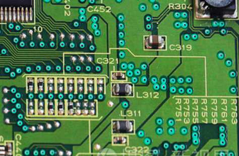
Multi-layer PCB line processing, and single layer and double layer no difference, the biggest difference in the hole process.
Lines are etched out, holes are drilled and then copper plated out, these do hardware development we all understand, do not repeat.
Multilayer circuit board, usually through the hole plate, first board, second board, second stack plate these several. Higher level such as the third level board, arbitrary layer interconnection board usually used very little, the price thief expensive, not to discuss.
Under normal circumstances, 8-bit single-chip microcomputer products with 2 layers of through hole plate; 32-bit single-chip level intelligent hardware, using 4-6 layers of through hole plate; Linux and Android level smart hardware, using 6-layer through hole to 8 first-stage HDI boards; Smart phone such compact products, generally use 8 layers of the first level to 10 layers of the second level circuit board.

The most common through-hole
There is only one perforation, from the first layer to the last layer. No matter the external line or the internal line, the hole is pierced, called through hole plate.
The circuit board is drilled through with a drill and copper plated in the holes to create a path.
Note that the inner diameter of the through hole is usually 0.2mm, 0.25mm and 0.3mm, but generally 0.2mm is much more expensive than 0.3mm. Because the drill bit is too thin and easy to break, the drill is also slower. The extra time and drill costs are reflected in the rising price of circuit boards.
Laser hole of high density board (HDI board)
This figure shows the laminated structure of 6 layers of 1 order HDI board. The two layers on the surface are laser holes with 0.1mm bore. The inner layer is a mechanical hole, equivalent to a 4-layer through hole plate, and the outside is covered with 2 layers.
Lasers can only Pierce fiberglass plates, not metal copper. So the outer surface punching will not affect the other lines inside.
After the laser hole is punched, the copper is plated, and the laser hole is formed.
Two layers of laser holes on a 2-stage HDI board
The picture above shows a 6 - layer 2 - order staggered HDI board. Usually we use 6 layers of 2 less, most of the 8 layers of 2. There are more layers here, same thing as six layers.
The so-called second order, there are two layers of laser holes.
The so-called wrong hole, is the two layers of laser holes are staggered.
Why stagger it? Because the copper plating is not satisfied, the hole inside is empty, so it can not be directly punched on the above, to stagger a certain distance, and then hit a layer of empty.
Six levels of second order is equal to four levels of first order plus two levels.
Eight levels of second order is equal to six levels of first order plus two levels.
Laminated plate technology is complex and the price is higher
The two layers of laser holes in the staggered plate overlap. The line will be tighter.
The inner laser hole needs to be electroplated and filled, and then the outer laser hole is made. The price is more expensive than the error hole.
Super expensive multi - layer laser hole - stacking of arbitrary - layer interconnectors
Each layer is a laser hole, and each layer can be connected together. Line the line however you want, punch the hole however you want.
Layout engineers think about it! No longer afraid not to draw!
Purchasing just think about crying, more than 10 times more expensive than the ordinary through hole plate!
So, only products like the iPhone are willing to use. Other phone brands, no one has ever heard of using any layer interconnection board.
summarize
Let's finish with a picture and compare it more closely.
Note the size of the hole and whether the pad for the hole is closed or open.
(2) It is a variant of the third laminated mode. Due to the addition of reference layer, it has better EMI performance, and the characteristic impedance of each signal layer can be well controlled:
1.Signal 1 component surface, microstrip wiring layer, good wiring layer
2.Ground stratum, good electromagnetic wave absorption ability
3.Signal 2 Cable routing layer. Good cable routing layer
4.Power layer, and the underlying strata constitute excellent electromagnetic absorption
5.Ground formation
6.Signal 3 Cable routing layer. Good cable routing layer
7.Power formation, with large power impedance
8.Signal 4 Microstrip cable layer. Good cable layer
(3) The best stacking mode, because the use of multi-layer ground reference plane has very good geomagnetic absorption capacity.
1.Signal 1 component surface, microstrip wiring layer, good wiring layer
2.Ground stratum, good electromagnetic wave absorption ability
3.Signal 2 Cable routing layer. Good cable routing layer
4.Power layer, and the underlying strata constitute excellent electromagnetic absorption
5.Ground formation
6.Signal 3 Cable routing layer. Good cable routing layer
7.Ground stratum, better electromagnetic wave absorption ability
8.Signal 4 Microstrip cable layer. Good cable layer
How to choose how many layers to use and how to use the layers depends on the number of signal networks on the board, device density, PIN density, signal frequency, the size of the board and many other factors. We should take these factors into consideration. The more the number of signal networks, the higher the density of the device, the higher the PIN density, the higher the frequency of the signal design should be adopted as far as possible. For good EMI performance it is best to ensure that each signal layer has its own reference layer.
Why are PCB design layers mostly even?
Mar 29,2023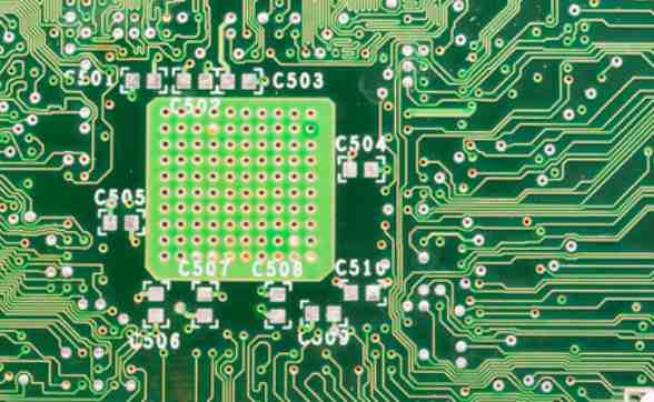


Just upload Gerber files, BOM files and design files, and the KINGFORD team will provide a complete quotation within 24h.