
Professional PCB manufacturing and assembly
Building 6, Zone 3, Yuekang Road,Bao'an District, Shenzhen, China
+86-13410863085Mon.-Sat.08:00-20:00

The selection and design of SMT surface-mounted components is a key part of the overall product design. In the SMT design stage, the packaging form and structure of surface assembled components should be determined according to the specific conditions of equipment and process and the overall design requirements. People talk about the development trend of printed circuit boards, printed circuit boards tend to high precision, high density and high reliability development direction, this is the development trend. Below, the SMT manufacturer will explain how to select components and how to improve PCB appearance quality in SMT processing.
1. How to improve PCB appearance quality
But on the other hand, the appearance of PCBS is becoming more and more strict. Like a solder shield on a printed circuit board... People talk about the development trend of printed circuit boards, printed circuit boards tend to high precision, high density and high reliability development direction, this is the development trend. But on the other hand, the appearance of PCBS is becoming more and more strict. Like the solder "sheath" on the printed circuit board, in addition to the requirements of a certain thickness and hardness, solvent resistance test and adhesion test standards, but also the surface color uniform and shiny, no garbage, no excess traces. It can be said that the appearance quality of flux resistance is not only the embodiment of the technical level and management level of the enterprise, but also directly affects the order of the enterprise. Therefore, how to improve the appearance quality of the printed circuit board flux resistance has become an urgent problem to be solved in every PCB factory.
Factors that affect the appearance quality of solder resistance
1. Printing:
Photosolder resistance printing ink screen printing process, blade flatness, environmental purification, screen printing using barrier tape and ink printing pressure, printing preparation before the plate will affect the appearance of the quality, according to the actual production situation, the most important factors are the first three, the blade is not easy to produce plane marks on the solder resistance printing surface; The purification is easy to form a barrier on the garbage surface; When using improper tape, easy to make ink gelatinous solvent and surface particles. Exposure: In the process of contact with welding ink, because the flux is not fully cured, the solder resistance layer and the solder paste together tend to produce impressions, which is the main reason affecting the appearance quality of the solder paste. Solder resistance ink through the development of general horizontal transfer type development, solder resistance is not fully cured, the developer drive wheel, press wheel and other easy to cause surface damage, roll marks, thus affecting the appearance of the solder resistance quality. In addition, incorrect exposure energy can also affect the gloss of the solder choke, but this can be controlled with a wedge meter.
2. After curing:
After curing, the temperature of the solder resistance is uneven, which is easy to lead to uneven color of the solder paste. When the temperature is too high, it will even cause local yellow and black, which affects the appearance of the solder. When screen printing solder ink, due to the uneven screen printing surface, after a period of screen printing, the surface of the scraper will become uneven, so there will be scratches on the surface of the solder resistance layer. Therefore, the operator must always pay attention to the surface condition, once found scraper marks, should immediately wipe the scraper to ensure smoothness. In order to obtain a printing board with good appearance quality, the cleanliness of the screen printing room plays a key role. All areas in contact with the printed circuit board (including workbench, screen frame, blotting paper, BLOCKOUTS tape) and the printed circuit board itself shall be dusted with drum dust. A clean room must be cleaned during turnaround. The cleaned room must be dressed in special clothing and hats, and in accordance with the regulations of the wind bath. At the same time, the protection of air purification around the factory is also crucial. If this happens, water can be sprayed around the plant regularly to remove dust. Development: The flux is not fully cured on the developing surface, leaving the impression of the roll easily. SMT patch processing: Therefore, it should be considered on equipment. The first driving roller must use soft material or roll coating, soft PVC "O" ring, roller, water extrusion roller made of soft rubber roller; Secondly, ensure the stability of the whole transmission system; This anti-roll mark is then produced by regular cleaning of the developing roller and a water squeezing roller to remove dirt from the roller and remove it. In order to improve the appearance quality of PCB solder resistance film, from the process, raw materials, equipment, operators and other aspects of comprehensive control, especially for screen printing parameters, exposure and development, after curing strict control. In this way, the appearance quality of the solder resistance layer of the printed circuit board can fully meet the needs of customers.

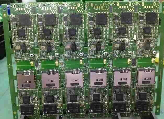
2. How to select components during SMT patchprocessing
First, choose the right package, mainly has the following advantages:
1. Effectively save PCB area and provide better electrical performance.
2. Provide good communication links to help dissipate heat and facilitate transmission and testing.
3. Protect the interior of the components from humidity and other environmental influences.
SMT surface-mounted components are divided into active and passive categories, and can be divided into gull wing type and "J" type according to pin shape.
1, passive devices Passive devices mainly include monolithic ceramic capacitors, tantalum capacitors and thick film resistors, rectangular or cylindrical shape.
2, active device surface mounted chip carrier has two categories: ceramic and plastic.
The advantages of ceramic chip package are: 1) good air tightness, good protection to the internal structure 2) short signal path, parasitic parameters, noise, delay characteristics are significantly improved 3) reduce power consumption. Plastic packaging is widely used in military and civilian production, with good cost performance. Its packaging form is divided into: small shape transistor SOT; Small shape integrated circuit SOIC; Plastic-sealed leaded chip carrier PLCC; Small shape J package; Plastic flat package PQFP.
How does PCBA improve product quality
Feb 12,2023


Just upload Gerber files, BOM files and design files, and the KINGFORD team will provide a complete quotation within 24h.