
Professional PCB manufacturing and assembly
Building 6, Zone 3, Yuekang Road,Bao'an District, Shenzhen, China
+86-13410863085Mon.-Sat.08:00-20:00

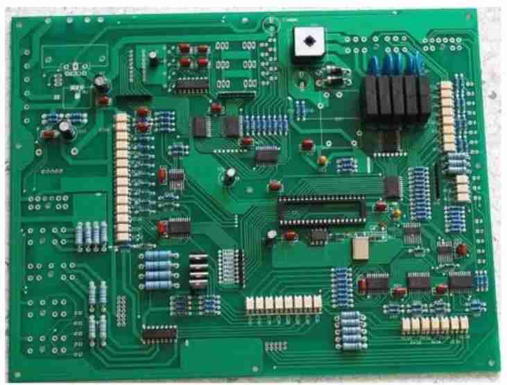
In SMT patch welding skills, there is a more common question, especially in the application of a new supplier's products in the early stage, or unstable production skills, more likely to occur such a question, through the use of customer cooperation, and through our many experiments, we ultimately analyze the causes of the attack of tin beads can have the following aspects, Below, the SMT processing manufacturer will explain how to solve the tin problem in SMT processing and how to carry out eye inspection in PCBA patch processing
1. How to inspect PCBA patch processing
Visual inspection is a process that must be carried out after PCBA patch processing. The main purpose of visual inspection is to provide timely feedback to the process in view of the poor appearance of PCB components and solder joints, so as to improve the yield of SMT process and product quality. Next, we will introduce how to inspect PCBA patch after processing.
1. Basic working conditions for visual inspection of PCBA patches after processing 1. Working conditions: Temperature: 18℃ to 28℃, humidity: 35% ~ 75%; 2. Operation object: all PCbas; 3. Operator: with certain general SMT and DIP welding status identification ability; 4. Job Responsibilities: Compare and screen bad welds, record bad marks, and fill in the corresponding forms.
2. Materials required for visual inspection after PCBA patch processing 1. PCBA: Quantity; 2. Label and record of defective products: 1 copy; 3. One ESD wrist strap. 4. Esd gloves: 1 pair. 5. Anti-static rotating rack: several.
Iii. Eye inspection Procedure after PCBA patch treatment 1. Wear anti-static clothes, anti-static wrist and gloves to sit; 2. Paste PCBA serial numbers in sequence for quality tracking. 3. Hold the PCBA with both hands and maintain a 45° tilt Angle. Scan key components and connectors line by line, from left to right and top to bottom, for bad welds. 4. Take the long side of PCBA as the axis and rotate at a certain Angle to observe whether the key components have adverse buoyancy, skew, welding leakage and welding leakage. 5. If a poorly welded component or connector is found and cannot be determined by itself, on-site management personnel should be consulted to confirm whether it is qualified and judgment should not be made at will. 6. When the defective product is found to be obviously defective, the label of the defective product is only a label. Note that the label of the defective product points to the defective arrow. 7. Turn over to the other side of PCBA, and focus on the welding quality of connector solder joints: whether there is uniformity of tin, leakage welding, less tin solder joints, cold welding, tin tip, dirt and other adverse phenomena, find abnormal adhesion defective labels, distinguish them, and put them on the shelf of defective products. 8. Inspect key parts visually several times, and place abnormal products on the shelf of qualified products. 9. Every 10 PCBA boards shall be conducted in groups and the relevant records shall be verified for completeness and transferred to the next process if there are no omissions. 10. Fill in the record list of defective products, and fill in the description of defective phenomena according to the serial number. 11. Defective products should be placed in the prescribed relatively fixed position, and clearly marked, do not confuse.

2. How to solve the tin problem in SMT patch processing
1. PCB board is not sufficiently preheated during reflow welding; 2. The setting of reflow welding temperature curve is not fair, and there is a large gap between the plate temperature and the welding zone temperature before entering the welding zone; 3. The solder paste failed to completely return to room temperature when it was taken out from the cold storage; 4. The tin paste is exposed to air for a long time after opening; 5, in the patch when tin powder splashed on the PCB board surface; 6. In the process of printing or transferring, there is oil or water sticking to the PCB board; 7, solder paste flux itself distribution is not fair, not easy to transpiration solvent or liquid additives or activators; The above top and the second reason, can also explain why the new replacement of the solder paste is easy to make such questions, the main reason is still the temperature curve is now set and used solder paste does not match, which requires customers in place of suppliers, must be asked to solder paste suppliers can be accustomed to the solder paste temperature curve; The third, fourth and sixth reasons can be the improper operation of the user; The fifth reason can be because the solder paste is stored improperly or beyond the shelf life of the solder paste failure caused by the solder paste is non-viscous or too low viscosity, when the patch constitutes the splash of tin powder; The seventh reason is the production skills of solder paste suppliers themselves. (3) after welding, there are more residues on the board surface: after welding, there are more residues on the PCB board surface is also a question that customers often reflect. The existence of more residues on the board surface not only affects the brightness of the board surface, but also has a certain impact on the electrical properties of PCB itself; The main reasons for the large amount of residue are as follows:
1, in the promotion of solder paste, do not know the customer's plate status and customer needs, or other causes of selection error; For example, the customer needs to use non-cleaning reside-free solder paste, and the solder paste manufacturer supplies rosin resin type solder paste, which causes the customer to reflect more residue after welding. In this respect, solder paste manufacturers are about to notice when promoting their products.
2, the content of rosin resin in the solder paste is too much or its quality is not good; This is about the skills of solder paste manufacturers. SMT is Surface Mounted Technology (short for Surface Mounted Technology). It is one of the most popular skills and skills in the electronic mounting profession. Electronic circuit Surface Mount Technology (SMT), known as surface mount or surface mounting skills. It is a kind of pin-free or short lead appearance assembly components (SMC/SMD, Chinese known as chip components) installed on the Printed Circuit Board (PCB) appearance or other substrate appearance, after reflow welding or immersion welding and other methods to weld assembly of the circuit installation skills.
How was the PCBA product developed
Feb 09,2023


Just upload Gerber files, BOM files and design files, and the KINGFORD team will provide a complete quotation within 24h.