
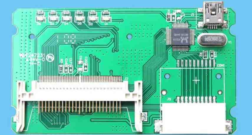
Professional PCB manufacturing and assembly
Building 6, Zone 3, Yuekang Road,Bao'an District, Shenzhen, China
+86-13410863085Mon.-Sat.08:00-20:00

Each copper foil is further classified into different grades according to its mechanical properties and applications. Electrolytic copper foil and forged copper foil are divided into four grades (Savage. 1992). Usually electrolytic copper foil is 1-4, used in rigid printed circuit boards. FPC Flexible circuit boards use all electrolytic and forged copper foils of grades 5-8. Typical stages 2,5,7 and 8 are used in flexible laminates. The following patch processing manufacturer Xiaobian to explain how to manufacture copper foil in circuit board FPC and how to optimize PCB design to meet the requirements of lead-free knowledge.
1. How to optimize PCB design to meet lead-free requirements
Lead-free environmental protection is a topic that PCB manufacturers and PCBA manufacturers talk about most and spend great efforts to improve. It is also a technical challenge for manufacturing. It has also spent a lot of manpower and material resources to carry out some research on PCB design, and has made the following progress: The main optimization design measures include:
1. Improvement of the specification of the encapsulation library
Due to the increase of lead-free welding temperature, it is necessary to consider the influence of the device pad on the temperature of the solder joint when building the library. At the same time, the reliability of welding and the heat resistance of the device should be tested to ensure that the size and shape of the pad, the size and shape of the solder resistance, the relationship between the steel mesh and the pad can meet the optimal welding temperature.
2. Design methods and details processing
Avoid the situation of welding monument, so the heating of the device should be considered in the design time, to ensure that each device is heated evenly. Therefore, we specially developed software to ensure the device heat balance.
3, the choice of surface treatment
Different surface treatment methods vary in cost and processing difficulty, so there are different surface treatment methods for different products. At the same time, some finishes have subtle differences in packaging or design. For example, when the surface treatment mode is OSP, the ICT test point needs to open the steel mesh. Other surface treatments do not have this requirement.
4. Identifier description
In the need of lead-free plate, need to add identification symbols for subsequent processing manufacturers to identify and deal with.

2. How to manufacture copper foil in circuit board FPC
In the flexible circuit board FPC, copper foil is used as the substrate, which is well known. However, very few people know how it is made. Copper foil is widely used in flexible circuit board FPC, but how to make it? Copper foils are manufactured by either calendering annealing or electrolysis, and these methods determine their mechanical paradoxes. Each copper foil is further classified into different grades according to its mechanical properties and applications. Electrolytic copper foil and forged copper foil are divided into four grades (Savage. 1992). Usually electrolytic copper foil is 1-4, used in rigid printed circuit boards. FPC Flexible circuit boards use all electrolytic and forged copper foils of grades 5-8. Typical stages 2,5,7 and 8 are used in flexible laminates.
1, electrolytic copper foil
Electrolytic copper foil is made by electroplating copper ions onto a cylindrical cathode, from which the foil is continually peeled off. Electrolytic copper foil is columnar grain structure. When the copper foil is bent, the particles separate, which makes the copper foil bend, its flexibility and rupture resistance is less than calendering annealed copper foil. The electrolytic process begins by separating copper from a solution of sulfuric acid, with temperature and agitation controlling the rate of decomposition. The shape and mechanical properties of copper foil may be controlled by using different types of additives. The copper solution is continuously injected into the electrolytic cell. Under the action of the current between the anode and cathode of the electrolytic cell, copper ions are precipitated from the chemical cell to the cathode surface. The cathode is a rotating cylindrical magnetic drum, one part of which is immersed in solution. As the cathode enters the solution, copper begins to deposit on the surface of the drum and is continuously electroplated until the drum leaves the solution. As the cathode continues to rotate, the copper foil is stripped away from the cathode. The rotation speed of the cathode drum determines the thickness of the copper foil, and the electrolytic process can produce copper foil of many thicknesses and widths. Raw copper foil products, whether forged or electrolyzed, also need to be processed in three stages. 1) Combined (fixed) treatment; This treatment usually involves the treatment of metallic copper/copper oxide, which increases the surface area of the copper and provides better wettability for the binder or resin. 2) Heat resistant treatment; This treatment enables the coppered laminate to withstand the high temperature environment during PCB manufacturing. 3) Stability treatment; Also known as passivation or oxidation resistance, this treatment is applied to both sides of the copper to prevent oxidation and staining. All stability treatments are based on aluminum alloys, and some manufacturers combine nickel, zinc, and other metals with lead. After treatment, the copper coil is cut to the required width and the cut core is wrapped in plastic film to prevent oxidation. The ductility of copper foil is as follows: 1) electrolytic copper foil: extension of 4%-40%. 2) Calendering annealed copper foil: extend 20%-45%. Copper foil is usually covered with a film made from polyimide or liquid polymerization of ficus. With this treatment, the conductor film provides long-term protection against corrosive environment and solder contamination.
2. Calendering annealed copper foil
Calendering annealed copper foil is made by first heating the copper chains and then feeding them into a series of rollers to reduce them to a specified thickness of copper foil. The rotation creates particle structures in the copper foil that look like lapped horizontal planes. Under pressure and temperature, copper particles of different sizes interact with each other to give the foil properties, such as ductility and hardness, while also producing a smooth surface. Compared with electrolytic copper foil, the copper foil produced by this production process can withstand more repeated bending. However, its disadvantages are higher cost and less choice of thickness and width of copper foil. Copper foil is usually covered with a film made from polyimide or liquid polymerization of ficus. With this treatment, the conductor film provides long-term protection against corrosive environment and solder contamination.
How should I choose the SMT plant
Feb 06,2023


Just upload Gerber files, BOM files and design files, and the KINGFORD team will provide a complete quotation within 24h.