
Professional PCB manufacturing and assembly
Building 6, Zone 3, Yuekang Road,Bao'an District, Shenzhen, China
+86-13410863085Mon.-Sat.08:00-20:00

Virtual welding is a common line fault, there are two kinds, one is in the process of circuit board production, due to improper production technology, when the unstable state; The other is that after long-term use of electrical appliances, some of the more serious heating parts, the welding spot at the welding foot is very easy to appear aging stripping phenomenon caused by. So how to distinguish circuit board welding problem? The following patch processing manufacturer Xiaobian to explain how to identify circuit board welding problems and BGA slices how to judge the welding quality of the relevant knowledge.
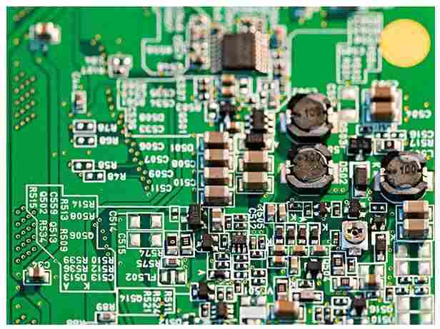
1. How to judge the welding quality of BGA slices
This is the picture of BGA solder after sliced by kingford's own products, which can be used as a textbook. Besides, there are typical double balls (HIP, Head-In-Pillow) and pictures of tin balls being pulled. Usually when you get a BGA slice photo, the first thing to judge is which side belongs to the packaging surface of BGA and which side belongs to the circuit board assembly surface. For this problem, my method is to judge from the thickness of copper foil. The thicker side of copper foil is usually the circuit board assembly surface, because the carrier board of BGA packaging is usually thinner than the circuit board of electronic assembly, so the thinner thickness of copper foil will be chosen.
Secondly, if the double ball phenomenon can be clearly seen (the following picture shows the typical shortcomings of HIP pseudo-cold welding), the larger side of the ball is usually the original tin ball on the carrier plate, because the volume of the BGA tin ball has been Reflow. On the other hand, the solder paste printed on PCB is only half of its original volume after a Reflow flux volatilization, so the spheres on BGA are usually larger. As for the size of welding Pad (pad) is not necessarily, it depends on whether your PCB layout Design adhere to the design of Cooper Define Pad Design (copper foil independent pad design). Then judging the quality of BGA welding, the following figure can clearly see the typical [double ball (HIP)] welding problem, those who do not understand can click the "HIP(Head-in-Pillow effect)" link for further discussion, 99% HIP should occur on the outer row of tin balls around the BGA. The cause is almost always the deformation and warping of BGA carrier plate or PCB after Reflow, and the deformation becomes smaller after the board is returned to temperature, but the molten tin has cooled, thus forming the appearance of two balls together.
HIP is a serious BGA solder defect, it is easy to pass through the factory testing procedures to the customer's hands, but after a period of use, the product will be sent back for repair due to problems. The second kind of bad BGA solder is the tin ball between HIP and normal solder. Do you know how to judge which side is PCB end? From below BGA solder ball and solder paste on the PCB has been completely fused together, because can't see the double ball, but the whole tin ball has been up and down spin and almost broken signs, observed on the surface of the PCB soldering tin can also find the ball contact with PCB soldering pad area is smaller, but also appears no ð « » long point of view, this is because the tin ball is the pull up
This kind of solder fracture should only be a matter of time, the client should be used when the vibration or switching process of thermal expansion and cold contraction, will accelerate its fracture. The welding of BGA tin ball in the following picture is acceptable. The ball can also be flattened to form horizontal oval solder, but it is still visible that the tin ball near the PCB end is somewhat pulled apart. In fact, a good solder ball shape should be like the picture below, the tin ball resembles a "lantern shape", the tin ball covers the entire PCB welding pad. However, sometimes the pads are designed to be covered with green oil, which makes the shape look more like the picture above.

2. How to identify the problem of circuit board welding
1. In the welding between the component foot of the circuit board and the solder, we can use the driver to press the solder welding edge to highlight the component foot. If the component foot can move, it is virtual welding.
2. If there is virtual welding between the solder joint and the pad, under normal circumstances, we can press down on the circuit board components, which will lead to the loosening of the circuit board components, that is virtual welding. In the circuit board, virtual welding is divided into two basic situations:
The first case: welding, facing this situation we need to use a multimeter to detect whether it is conductive, can not easily find the problem, if there is vibration or external influence, because the welding surface is small, easy to occur dewelding, it is easy to find at this time.
The second situation: the circuit boardis completely not welded, simple understanding is that the solder and solder joint is not welded, just simple contact. In this case, the first thing we need to do is to see if the cleaning of the welding surface is enough. If the cleaning is good, the multimeter also shows the conduction. Cleaning is not good, if there are oxides on the surface may be impenetrable, at this time the multimeter can not be very accurate check out the welding.
Solution: First of all, we need to apply a certain external force to the components to be welded. If there is no loosening, it can be judged that there is no virtual welding. In addition, can directly observe the solder joint, virtual welding of the solder edge and welding surface is not very good fit, generally can be seen, two methods, basically can be found out, at the same time, for not easy to judge, can take the method of welding to avoid, welding a solder joint quickly. To avoid virtual welding, mainly to the welding surface cleaning and tin, cleaning is best not to use solder paste, because contains acid material, may corrosion element pin, resulting in virtual welding, after cleaning oxide, to solder surface first on tin, and then welding is easy, is not easy to produce virtual welding.a


Just upload Gerber files, BOM files and design files, and the KINGFORD team will provide a complete quotation within 24h.