
Professional PCB manufacturing and assembly
Building 6, Zone 3, Yuekang Road,Bao'an District, Shenzhen, China
+86-13410863085Mon.-Sat.08:00-20:00

As an excellent designer, only by knowing some special requirements of SMT process in advance can we maintain high quality and high efficiency in the SMT production process. Because in the SMT process of FPC, the flatness of the board itself is very high; In addition, the spacing, MARK point setting, the size of the board and so on will affect the quality and efficiency of SMT, so as a design engineer of FPC manufacturers should understand more about some special requirements of SMT combined with the FPC process ability before the comprehensive consideration of design, do not pay attention to one or the other, otherwise the future is endless. Next, kingford will explain how to maintain high efficiency in SMT patchprocessing and how to solve the problem of substrate size change.
1. How to solve the problem of changing the size of the substrate
Reasons for the change in the size of the substrate in the process of circuit board production:
(1) Changes in substrate size caused by differences in longitude and latitude directions; Because the fiber direction is not paid attention to during shearing, the shear stress remains in the substrate. Once released, it directly affects the shrinkage of the substrate size.
⑵ The copper foil on the surface of the substrate is etched away, and the size changes when the stress is removed.
(3) Brush plate due to the use of excessive pressure, resulting in compressive tensile stress resulting in deformation of the substrate.
(4) The resin in the substrate is not fully cured, leading to size changes.
⑸ The multilayer plate in particular before lamination, storage conditions are poor, so that the thin substrate or semi-cured sheet moisture absorption, resulting in poor dimensional stability.
⑹ laminate by pressing, excessive flow caused by glass cloth deformation.
The solution to the change of substrate size in the process of circuit board production:
(1) Determine the change law of longitude and latitude direction according to the shrinkage rate on the negative to compensate (light painting before the work). At the same time, it is processed in the direction of fiber or according to the character mark provided by the manufacturer on the substrate (generally, the vertical direction of the character is the vertical direction of the substrate).
⑵ In the design of the circuit should try to make the whole board surface distributed evenly. If this is not possible it is also necessary to leave the transition segment in space (does not affect the circuit position of the main). This is due to the difference of the warp and weft density in the glass fabric structure, resulting in the difference of the warp and weft strength of the plate.
(3) Should be used to test brush, so that the process parameters in the best state, and then rigid plate. For thin substrate, chemical cleaning process or electrolytic process should be used when cleaning.
(4) Take baking method to solve. In particular, the drilling was baked before the temperature of 120℃ for 4 hours to ensure that the resin solidified and reduce the deformation of the size of the substrate due to the influence of heat and cold.
⑸ The inner layer of oxidized substrate must be baked to remove moisture. And the treated substrate is stored in a vacuum drying oven, so as not to absorb moisture again.
The process pressure test, adjust the process parameters and then press. At the same time can also be based on the characteristics of the semi-cured sheet, choose the appropriate amount of flow glue.

2. How to maintain high efficiency in SMT patch processing
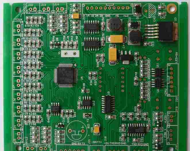
1. The Mark point is round or square, with a diameter of 1.0mm, depending on the equipment of SMT. The copper area from the Mark point to the surrounding area should be larger than 2.0mm, and crease, dirt and copper exposure are not allowed at the Mark point;
2. The four corners of each large board must have a Mark point or two Mark points in the diagonal, the Mark point from the edge should be greater than 5mm;
3. Each small board must have two Mark points; 4. According to the specific equipment and efficiency evaluation, FPC assembling board is not allowed to have "X" board;
5. When repairing the board, the key areas should be firmly glued to the board with wide adhesive paper, and then check the film. If the repairing board is uneven, it is necessary to press again and check the film again;
6. 0402 component pad spacing is 0.4mm; The spacing between 0603 and 0805 components is 0.6mm; The pad is best treated into a square;
7. In order to avoid the small area of FPC board due to punching subsidence, punching from the bottom direction; 8. After the FPC board is made, it must be baked and vacuum packed; Before SMT goes on line, it is best to pre-bake;
9. The best size of the board is less than 200mmX150mm; 10. There shall be four positioning holes for SMT fixture at the edge of the assembly plate, the aperture of which is 2.0mm;
11. The minimum distance between the edge element of the plate and the edge of the plate is 10mm; 12. Splicing board distribution as far as possible, each small board is distributed in the same direction;
13. The gold finger area of each small plate (i.e., hot pressing end and weldable end) is pieced together to avoid the gold finger eating tin in SMT production;
14. The minimum distance between Chip component pads is 0.5mm.
Engineering designers and technicians have probably had such experience: after the completion of FPC production, all the components need to be welded on SMT; The problem is that a good designer can maintain high quality and efficiency in the SMT production process by knowing some special requirements of the SMT process in advance. Because in the SMT process of FPC, the flatness of the board itself is very high; In addition, the spacing, MARK point setting, the size of the board and so on will affect the quality and efficiency of SMT, so as a design engineer of FPC manufacturers should understand more about some special requirements of SMT combined with the FPC process ability before the comprehensive consideration of design, do not pay attention to one or the other, otherwise the future is endless.
How to judge the welding quality of BGA slices
Feb 06,2023


Just upload Gerber files, BOM files and design files, and the KINGFORD team will provide a complete quotation within 24h.