
Professional PCB manufacturing and assembly
Building 6, Zone 3, Yuekang Road,Bao'an District, Shenzhen, China
+86-13410863085Mon.-Sat.08:00-20:00

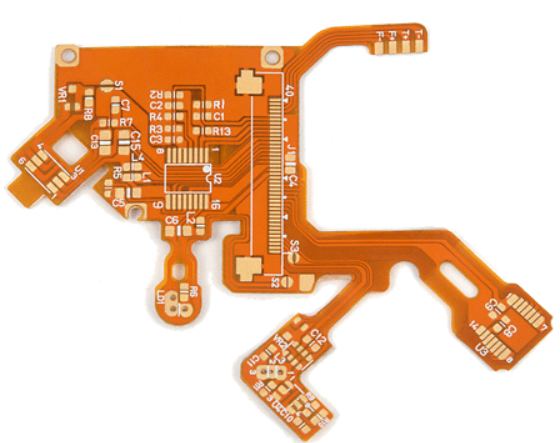
With the product is thin and short, the application of FPC is more and more, and some of them replace the traditional PCB, but today's FPC no matter how the progress is still connected to the PCB, and its interface design is still based on the connector, how to design FPC can better meet the needs of factory assembly is often important. Below, KingFord Xiaobian will explain how PCB design meets the requirements of factory assembly and how to copy the board.
How to copy the board
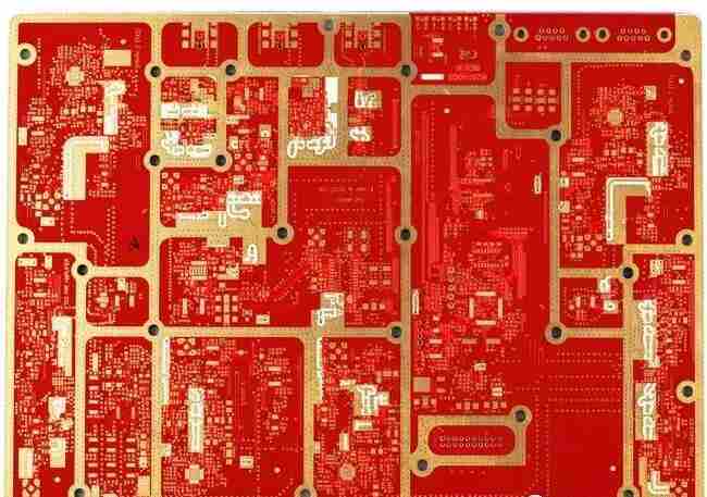
In the absence of electronic document production materials, only circuit board sample, in order to shorten the development time, save development costs, using the sample to copy board proofing is a very affordable way. The following KingFord introduces the method of PCB copying board:
The first step is to get a PCB. Firstly, record the model, number and position of all components on the paper, especially the direction of the diode, the three-stage tube and the direction of the IC notch. It is best to take two pictures of the location of the key parts with a digital camera. Now the circuit board is getting more and more advanced on the top of the bipolar tripolar some don't notice you can't see.
The second step is to remove all the devices and remove the tin from the PAD hole. The PCB is cleaned with alcohol and placed in a scanner, which scans with slightly higher pixels to get a sharper image. Then the top and bottom layers are lightly polished with gauze paper until the copper film shines, put them in the scanner, start PHOTOSHOP, and sweep the two layers in color separately. Note that PCB must be placed horizontally and vertically in the scanner, otherwise the scanned image cannot be used.
The third step is to adjust the contrast and brightness of the canvas, so that the part with copper film is in strong contrast with the part without copper film, then turn the subdrawing to black and white, check whether the lines are clear, if not, repeat this step. If it is clear, save the picture as black and white BMP format files TOP.BMP and BOT.BMP. If there is any problem with the picture, you can use PHOTOSHOP to repair and correct it.
The fourth step is to convert the two BMP files into PROTEL files respectively, and transfer two layers into PROTEL. If the positions of PAD and VIA after two layers basically coincide, it indicates that the previous steps have been done well. If there is any deviation, repeat the third step. So pcb copying board is a very patient work, because a little problem will affect the quality and the degree of matching after copying board.
Step 5, convert the BMP of the TOP layer to the TOP.PCB, be careful to convert to the SILK layer, which is the yellow layer. Then you trace the line on the TOP layer and place the device according to the drawing of step 2. Delete the SILK layer when you are done. Repeat until all layers are drawn.
In the sixth step, TOP.PCB and BOT.PCB are transferred into PROTEL, and it is OK to combine into a figure.
Step 7: Use a laser printer to print the TOP LAYER and BOTTOM LAYER onto the transparent film (1:1 ratio), place the film on the PCB, compare and see if it's wrong, if it's right, you're done. A copy board equal to the original was created, but it was only half done.
But also to test, test board electronic technology performance is not and the original board. If one ocean is really done. Remarks: If it is the multilayer board but also carefully polished to the inside of the inner layer, at the same time repeat the third to the fifth step of copying board steps, of course, the name of the graph is different, according to the number of layers, the general double panel copying board is much simpler than the multilayer copying board, multi-layer copying board is easy to appear the situation is not correct, So the multilayer board copy board to be particularly careful and careful (which internal through holes and non-through holes are easy to appear problems).

How are PCBS designed to meet factory assembly requirements
In the early days, KingFord always thought that the design emphasis of FPC was to stiffener layout and stiffener thickness under the golden finger. It would not be too thick for the FPC to be inserted into the connector or too thin and loose. Later, I occasionally found that FPC would fracture, especially in the HotBar operation, I found that it is not possible to design the section of all materials stacked on the same vertical surface, so as to concentrate the stress. Then I found that the copper foil of FPC has the so-called difference between rolled copper (RA) and electrolytic copper (ED). The selection of the wrong copper foil will affect the life of FPC bending times, and then it was found that more than two layers of rolled copper in the conduction process will still use copper plating, so that the characteristics of rolled copper almost disappeared. As electronic products get smaller and smaller, the FPC connector gets smaller and smaller. Although the FPC does not get smaller, it feels bigger, because it replaces some of the functions of the PCB, and the circuit seems to get denser. In addition, the parts adjacent to the FPC connector become more and more close. Relatively, it is becoming more and more difficult to assemble the FPC properly. Does your company have any special design to help operators to ensure that the FPC is installed and positioned? What's a foolproof design or foolproof that helps operators foolishly install FPCS? The following FPC designs can be seen in many mobile phone designs, but I just put them up for you to see what else you can discuss.
1. Design the FPC installation indicator line After the FPC connector is covered, the FPC installation indicator line is just in the edge position, which is conducive to determine whether the FPC is installed to the location. The installation of indicator line on the front and back of the FPC can help the operator to determine whether the FPC has been correctly installed to the positioning. The more particular will require the design of two lines. When the FPC is installed to the positioning, the first indicator line will be covered by the connector, and the second indicator line will be left outside the connector, so that the operator can more clearly judge whether there is no deviation. KingFord think that in fact there is a indicating line is enough, this indicating line is best in the connector cover can also see a little bit of it.
2. Extend the length of the backless adhesive reinforcing plate. The backless adhesive reinforcing plate can make the FPC easy to be grabbed, so that the operator can install the FPC into the connector more smoothly.
3. Design Extra Wings for a small FPC Add an extra TAB on either side of the FPC near the goldfinger to make it easy to grab the FPC board and attach it to the connector, or design a "pickpocket" gadget to grab the ears and slide the FPC into the connector.
How to ensure safety in patch processing
Feb 03,2023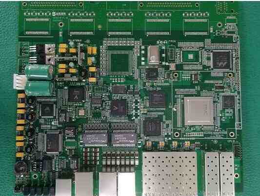


Just upload Gerber files, BOM files and design files, and the KINGFORD team will provide a complete quotation within 24h.