
Professional PCB manufacturing and assembly
Building 6, Zone 3, Yuekang Road,Bao'an District, Shenzhen, China
+86-13410863085Mon.-Sat.08:00-20:00

Differences among SMT, PCB, PCBA and DIP
Surface mount is one of the basic components of electronic components It is called surface mount technology (or surface mount technology). It is divided into no lead or short lead It is a circuit component connected by welding and assembled by reflow welding or dip welding Technology is also the most popular technology and process in the electronic assembly industry
Features: Our substrate can be used for power supply, signal transmission, heat dissipation and structure.
Features: It can withstand the temperature and time of curing and welding.
The flatness meets the manufacturing technical requirements.
Applicable to rework.
Manufacturing technology applicable to substrate.
Low permittivity and high resistance.
The commonly used materials of our products are healthy and environment-friendly epoxy resin and phenolic resin, which have good flame retardancy, temperature characteristics, mechanical and dielectric efficiency and low cost.
The above is rigid substrate curing.
Our products also have flexible substrates for space saving, folding or turning and moving. They are made of very thin insulating plates and have good high-frequency efficiency.
I think the characteristics of the substrate are small lead and spacing, large thickness and area, better thermal conductivity, harder mechanical efficiency and better stability. I think the mounting technology on the substrate is the power efficiency, reliability and standard parts.
We not only have fully automatic and integrated operations, but also have the dual assurance of manual audit, machine audit and manual audit, and the product pass rate is up to 99.98%.
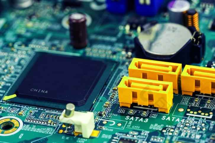
Secondly, the printed circuit board is the most important electronic component. Generally, conductive patterns made of printed circuits, printed elements or a combination of both on insulating materials according to a predetermined design are called printed circuits. The conductive pattern that provides electrical connection between components on the insulating substrate is called printed circuit board (or printed circuit board), which is an important support of electronic components and a carrier that can carry components.
Printed circuit board
I think we usually open the computer keyboard and see a soft film (flexible insulating substrate), which is printed with a silver white (silver paste) conductive pattern and a healthy bit pattern. Since this pattern is obtained by the general screen printing method, we call this printed circuit board flexible silver paste printed circuit board. The main computer boards, graphics cards, network cards, data machines, sound cards and printed circuit boards on household appliances that we see in the computer city are different.
The substrate used is made of paper (usually used for one side) or glass cloth (usually used for both sides and multiple layers), pre impregnated with phenolic resin or epoxy resin, and the surface layer is laminated with copper film on one side or both sides, and then laminated and cured. This kind of circuit board copper clad material is called rigid board. Then make a printed circuit board, which we call rigid printed circuit board.
We call single-sided printed circuit board single-sided printed circuit board and double-sided printed circuit board double-sided printed circuit board. The printed circuit board formed by the metallization of double-sided interconnects is called double-sided board. If one double side of a printed circuit board is used as the inner layer, two single sides are used as the outer layer, or two double sides are used as the inner layer, and two single sides are used as the outer layer, the positioning system and insulation bonding materials are alternately combined, and the printed circuit board with conductive patterns interconnected according to the design requirements becomes a four layer or six layer printed circuit board, also known as a multilayer printed circuit board.
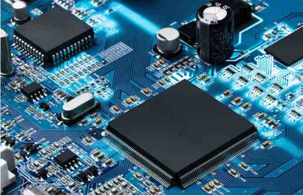
Third, PCBA is one of the basic components of electronic components. The whole process of PCB insertion through surface mount technology (SMT) and DIP parts is called PCBA process. In fact, it is a PCB with patches. One is finished board, and the other is bare board.
PCBA can be understood as a finished circuit board, that is, after all the processes of the circuit board are completed, it can be counted as PCBA. Due to the continuous miniaturization and refinement of electronic products, most current circuit boards are attached with corrosion inhibitors (laminates or coatings). After exposure and development, the circuit board is made by etching.
In the past, due to the low assembly density of PCBA, the understanding of cleaning was not enough. Some people believed that the flux residue was non-conductive and benign, and would not affect the power efficiency.
Today's electronic components tend to be smaller, even smaller equipment or smaller spacing. The pins and pads are getting closer. Now, the gap is getting smaller and smaller, and pollutants may get stuck in the gap. This means that relatively small particles may remain between the two gaps. The undesirable phenomenon causing short circuit.
In recent years, the electronic assembly industry has become increasingly aware of and calls for cleaning, not only for products, but also for environmental requirements and protection of human health. There are many suppliers of cleaning equipment and solutions. Cleaning has become one of the main contents of technical exchanges and discussions in the electronic assembly industry.
4. DIP is one of the basic components of electronic components. It is called dual in line packaging technology, which refers to the integrated circuit chips packaged in dual in line form, and is also used in most small and medium-sized integrated circuits. The number of pins shall not exceed 100.
DIP capacitor
CPU chips with DIP packaging technology have two rows of pins, which need to be inserted into chip slots with DIP structure.
Of course, it can also be directly inserted into the circuit board with the same number of welding holes and geometric shapes for welding.
DIP packaging technology should be particularly careful when plugging from the chip socket to avoid damage to the pins.
Features: Multilayer ceramic dual in-line welding, single-layer ceramic dual in-line welding, lead frame in-line welding (including microcrystalline glass sealing type, plastic packaging structure type, ceramic low melting point glass packaging type), etc.
DIP parts are a link in the electronic manufacturing process. There are manual parts and artificial intelligence machine parts. Inserts the specified data into the specified location. Manual parts must be wave soldering to solder electronic components on the circuit board. For inserted components, check whether they are inserted incorrectly or missing.
DIP plug-in post weld treatment is a very important process in welding PCBA patch Its processing quality directly affects the function of PCBA board, and its importance is very important Due to the limitation of process and data, some parts cannot be welded with wave soldering machine. Post welding treatment is required, but it can only be done manually
This also reflects the importance of DIP components in electronic components. Only by paying attention to details can it be perfect.
Each of the four electronic components has its own advantages, but they complement each other and form a series of production processes. Only by checking the quality of the products produced, can the majority of users and customers appreciate our intentions.
Surface mount is one of the basic components of electronic components It is called surface mount technology (or surface mount technology). It is divided into no lead or short lead It is a circuit component connected by welding and assembled by reflow welding or dip welding Technology is also the most popular technology and process in the electronic assembly industry
Features: Our substrate can be used for power supply, signal transmission, heat dissipation and structure.
Features: It can withstand the temperature and time of curing and welding.
The flatness meets the manufacturing technical requirements.
Applicable to rework.
Manufacturing technology applicable to substrate.
Low permittivity and high resistance.
The commonly used materials of our products are healthy and environment-friendly epoxy resin and phenolic resin, which have good flame retardancy, temperature characteristics, mechanical and dielectric efficiency and low cost.
The above is rigid substrate curing.
Our products also have flexible substrates for space saving, folding or turning and moving. They are made of very thin insulating plates and have good high-frequency efficiency.
I think the characteristics of the substrate are small lead and spacing, large thickness and area, better thermal conductivity, harder mechanical efficiency and better stability. I think the mounting technology on the substrate is the power efficiency, reliability and standard parts.
We not only have fully automatic and integrated operations, but also have the dual assurance of manual audit, machine audit and manual audit, and the product pass rate is up to 99.98%.
Secondly, the printed circuit board is the most important electronic component. Generally, conductive patterns made of printed circuits, printed elements or a combination of both on insulating materials according to a predetermined design are called printed circuits. The conductive pattern that provides electrical connection between components on the insulating substrate is called printed circuit board (or printed circuit board), which is an important support of electronic components and a carrier that can carry components.
Printed circuit board
I think we usually open the computer keyboard and see a soft film (flexible insulating substrate), which is printed with a silver white (silver paste) conductive pattern and a healthy bit pattern. Since this pattern is obtained by the general screen printing method, we call this printed circuit board flexible silver paste printed circuit board. The main computer boards, graphics cards, network cards, data machines, sound cards and printed circuit boards on household appliances that we see in the computer city are different.
The substrate used is made of paper (usually used for one side) or glass cloth (usually used for both sides and multiple layers), pre impregnated with phenolic resin or epoxy resin, and the surface layer is laminated with copper film on one side or both sides, and then laminated and cured. This kind of circuit board copper clad material is called rigid board. Then make a printed circuit board, which we call rigid printed circuit board.
We call single-sided printed circuit board single-sided printed circuit board and double-sided printed circuit board double-sided printed circuit board. The printed circuit board formed by the metallization of double-sided interconnects is called double-sided board. If one double side of a printed circuit board is used as the inner layer, two single sides are used as the outer layer, or two double sides are used as the inner layer, and two single sides are used as the outer layer, the positioning system and insulation bonding materials are alternately combined, and the printed circuit board with conductive patterns interconnected according to the design requirements becomes a four layer or six layer printed circuit board, also known as a multilayer printed circuit board.
Third, PCBA is one of the basic components of electronic components. The whole process of PCB insertion through surface mount technology (SMT) and DIP parts is called PCBA process. In fact, it is a PCB with patches. One is finished board, and the other is bare board.
PCBA can be understood as a finished circuit board, that is, after all the processes of the circuit board are completed, it can be counted as PCBA. Due to the continuous miniaturization and refinement of electronic products, most current circuit boards are attached with corrosion inhibitors (laminates or coatings). After exposure and development, the circuit board is made by etching.
In the past, due to the low assembly density of PCBA, the understanding of cleaning was not enough. Some people believed that the flux residue was non-conductive and benign, and would not affect the power efficiency.
Today's electronic components tend to be smaller, even smaller equipment or smaller spacing. The pins and pads are getting closer. Now, the gap is getting smaller and smaller, and pollutants may get stuck in the gap. This means that relatively small particles may remain between the two gaps. The undesirable phenomenon causing short circuit.
In recent years, the electronic assembly industry has become increasingly aware of and calls for cleaning, not only for products, but also for environmental requirements and protection of human health. There are many suppliers of cleaning equipment and solutions. Cleaning has become one of the main contents of technical exchanges and discussions in the electronic assembly industry.
4. DIP is one of the basic components of electronic components. It is called dual in line packaging technology, which refers to the integrated circuit chips packaged in dual in line form, and is also used in most small and medium-sized integrated circuits. The number of pins shall not exceed 100.
DIP capacitor
CPU chips with DIP packaging technology have two rows of pins, which need to be inserted into chip slots with DIP structure.
Of course, it can also be directly inserted into the circuit board with the same number of welding holes and geometric shapes for welding.
DIP packaging technology should be particularly careful when plugging from the chip socket to avoid damage to the pins.
Features: Multilayer ceramic dual in-line welding, single-layer ceramic dual in-line welding, lead frame in-line welding (including microcrystalline glass sealing type, plastic packaging structure type, ceramic low melting point glass packaging type), etc.
DIP parts are a link in the electronic manufacturing process. There are manual parts and artificial intelligence machine parts. Inserts the specified data into the specified location. Manual parts must be wave soldering to solder electronic components on the circuit board. For inserted components, check whether they are inserted incorrectly or missing.
DIP plug-in post weld treatment is a very important process in welding PCBA patch Its processing quality directly affects the function of PCBA board, and its importance is very important Due to the limitation of process and data, some parts cannot be welded with wave soldering machine. Post welding treatment is required, but it can only be done manually
This also reflects the importance of DIP components in electronic components. Only by paying attention to details can it be perfect.
Each of the four electronic components has its own advantages, but they complement each other and form a series of production processes. Only by checking the quality of the products produced, can the majority of users and customers appreciate our intentions.
Advantages of SMD parts and poor PCBA welding
Dec 28,2022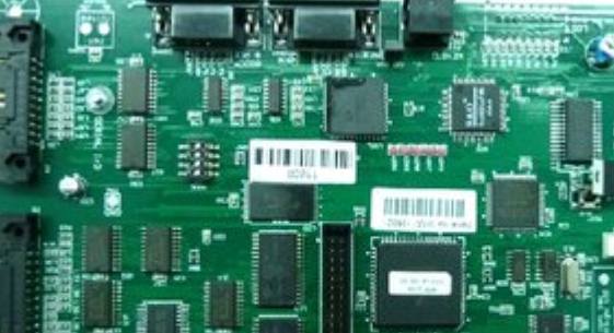


Just upload Gerber files, BOM files and design files, and the KINGFORD team will provide a complete quotation within 24h.