
Professional PCB manufacturing and assembly
Building 6, Zone 3, Yuekang Road,Bao'an District, Shenzhen, China
+86-13410863085Mon.-Sat.08:00-20:00

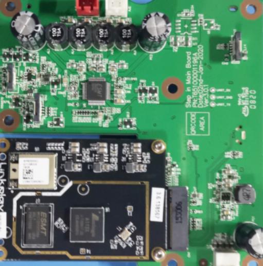
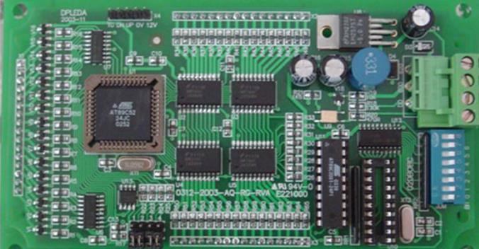
Information on PCB copper plating process and SMT chip
PCB copper wire cladding process
Copper clad laminate plays a very important role in PCB production. Sometimes, the success or failure of CCL is related to the quality of the whole circuit board. The so-called copper coating is to fill the blank space of PCB substrate with solid copper.
There are two methods for copper coating: large area copper coating and grid copper coating. Large area copper plating adds current and mask. However, if wave soldering is used, the circuit board may lift or even bubble. The grid copper can reduce the heating surface of copper and play an electromagnetic shielding role to a certain extent. However, the grid consists of traces. If the width of traces is not appropriate, interference signals will be generated.
Advantages of PCB Copper Cladding Process
The copper coating in SMT wafer processing has many advantages for PCB, such as improving noise resistance, reducing potential difference, reducing grounding impedance, improving anti-interference capability, reducing voltage drop, improving power efficiency, and connecting to the ground to reduce circuit area, heat dissipation and impedance reduction. Copper clad laminate has many advantages. Pay attention to the following items during operation:
2. The crystal oscillator in the circuit is a high-frequency emission source. The nearby copper clad plate surrounds the crystal oscillator, and then the shell of the crystal oscillator is grounded separately.
3. There should be no sharp angle, that is, the angle is greater than 180 °, or a transmission antenna will be formed.
SMT patch processing of patch data
In the process of electronic product chip processing, there are many factors that affect the product quality, such as the chip processing equipment, technology, process and PCB design that we often know, and the selection of chip processing data also has a great impact on the product quality. Selecting appropriate substrate information can effectively improve product efficiency and ensure product quality. So, what is the patch data in the patch processing? Let's learn about Jingbang Technology.
There are two main types of patch data in patch processing. One is organic patch data represented by metal based patch; The other is inorganic patch data represented by ceramic patch and copper plated ceramic shaft patch.
1. Metal patch: use 0.3mm-2. Omm thick metal plate, such as aluminum plate, steel plate, copper plate, epoxy prepreg and copper foil. The metal plate can realize large-area chip processing, and has the following performance characteristics:
(1) Good mechanical efficiency: metal based patch has higher mechanical strength and toughness, superior to rigid data patch, and can be used for large-area patch processing, and can bear the installation of overweight parts. In addition, the metal substrate patch also has high dimensional stability and flatness.
(2) Good heat dissipation efficiency: due to the direct contact between the metal sheet and the prepreg, it has good heat dissipation efficiency. The metal patch is used for patch processing. The metal patch can play a role in heat dissipation during processing. The heat dissipation capacity depends on the data and thickness of the metal sheet and the thickness of the resin layer. Of course, power efficiency, such as power intensity, should also be considered when considering heat dissipation efficiency.
(3) Shielding electromagnetic wave: In high-frequency electronic circuits, preventing electromagnetic wave radiation has always been a concern of designers. The metal substrate patch can be used as a mask to mask electromagnetic waves.
2. Electronic functional ceramic materials: electronic functional ceramics are one of the basic materials of microelectronic devices, and have the following advantages:
(1) New packaging materials for large-scale integrated circuits and new high-performance insulating ceramics for high-frequency insulation;
(2) It can replace imported new microwave ceramics, dielectric ceramics and ferroelectric ceramics for ceramic capacitors;
(3) Special electronic ceramic materials and products for high-performance chip components of large-scale integrated circuits.
There are many types of SMT patch processing for patch data in It is necessary to select the appropriate patch material according to the actual use and processing conditions to ensure the final product molding quality


Just upload Gerber files, BOM files and design files, and the KINGFORD team will provide a complete quotation within 24h.