
Professional PCB manufacturing and assembly
Building 6, Zone 3, Yuekang Road,Bao'an District, Shenzhen, China
+86-13410863085Mon.-Sat.08:00-20:00

Overview and sharing of PCBA electrical stress testing methods
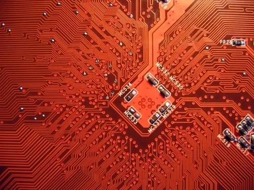
Quality control in mass production and prototyping has a set of important common tasks: the need for PCB testing. The specific test set you need to perform in PCBA depends on its application field, ideal service conditions, and of course, the relevant industry standards of your product. During the manufacturing and assembly process, you may be required to perform some basic tests and inspections on your PCB/PCBA. It is recommended to perform these tests at least to ensure continuity and accurate assembly, and simply find any obvious defects that may require rework.
High reliability applications may require more than simple electrical testing and inspection, whether in the manufacturing/assembly process, once the prototype is in the hands of the design team, and/or by an external testing laboratory. Electrical stress testing is only one of the possible tests that should be performed in high reliability components to ensure that the PCBA can withstand harsh electrical conditions.
Fundamentals of Electrical Pressure Testing
First of all, when it comes to things like testing, new designers may think that they have forgotten something, or they must plan some extreme tests before they can accept the circuit boards provided by the manufacturer. You will carry out a lot of functional tests, but you don't need to worry about the stress limits in the specific quantized circuit boards, unless you are reviewed by a standards organization (such as UL), your products have regulatory requirements, and you are transitioning to high capacity. The circuit board assembly and circuit board processing manufacturers explain the overview of PCBA electrical stress testing methods.
If you are prototyping, or if you are producing only a small number of disposable boards, do not over think about this. Hobbies, simple prototypes, demo board projects, or one-off projects are generally not suitable for electrical pressure testing. There are some exceptions with a quantity of 1, such as highly specialized aerospace products (satellites, unmanned aerial vehicles, etc.). If your circuit board will not be deployed in areas or conditions where there is a risk of extreme electrical stress, you may not need to perform electrical stress testing.
By the way, what is the current new technology of electrical pressure testing, and what exactly is "pressure"? Some of the main stress testing methods may fall into the following areas:
Electrical overstress test
Electrostatic discharge (ESD) test
Environmental pressure screening
Accelerated life testing
The idea is to find out the problems that will cause unexpected failures in the board of directors, or simply quantify when the board of directors will fail (or both). Although other quality control tests may be conducted during the manufacturing process, we will temporarily focus on the above list.
Electrical overload (EOS) test
This is sometimes confused with ESD, because they are all forms of overstress on components. The EOS test is probably the simplest electrical pressure test that can be performed: the components are basically overloaded, and the DUT is monitored until the equipment fails. This is usually performed at the wafer level or at the individual device level, just to quantify when the device will fail and its failure mechanism. The circuit board assembly and circuit board processing manufacturers explain the overview of PCBA electrical stress testing methods.
If you are looking at ratings in the data table, you will see recommendations based on EOS test results for individual components. These ratings are defined with a margin of safety, so you may be able to exceed them. What you do not see is an electrical overload at the system level. This is where you need to manually overload the system at each interface and power supply, and you need to monitor performance or output to ensure that the device can withstand any expected overload.
Electrostatic discharge (ESD) test
This test is just like its name: it tests the degree to which PCBA can withstand ESD events. When an ESD event occurs, your PCBA will interact with a very strong electrical pulse, which may reach more than 10000 V and more than a few amperes of current. If such events are not transferred back to safety ground in the system, components may be damaged. The ESD circuit is designed to absorb and/or transfer ESD pulses away from components and into a safe grounded area in the system. Some digital interfaces (such as IEEE 802.3 standard on Ethernet PHY) have their own ESD requirements, which must be met at the component level.
JEDEC distinguishes ESD at the component level and system level. PCB designers need to consider what will happen at the system level, because this is the area they can control.
This figure shows where system level ESD may occur. Exposed IO and connectors are obvious locations where ESD events can transmit electrical pulses to the system and may damage components.
System level ESD events occur in PCBA, which may affect multiple components, resulting in one of the following results:
There is no problem if the system continues to work
The system has failed/locked (soft failure), but there is no physical failure.
Physical damage to the system (hard failure)
Various industry standards beyond IPC standards put forward requirements on the ability of equipment to withstand electrostatic discharge. The specific test method depends on the standards adopted by your product (such as IEC 62368-1/IEC 61000, ISO 10605 for automobiles, DO-160 for avionics, etc.). Refer to the relevant security standards of your product and industry to determine the level of ESD protection your product requires.
Environmental Stress Screening (ESS) Test
These tests are designed to closely simulate the ideal deployment environment for devices. ESS testing may involve application thermal cycling, drop testing, vibration testing, thermal/mechanical shock testing, and any other environmental or mechanical exposure to which the equipment is expected during operation. More specialized testing methods may involve crash testing, pressure and humidity testing, or even altitude testing. Highly reliable systems need to withstand all these environmental factors during electrical operation, so a variety of tests are usually required to ensure reliability.
Functional tests are also performed before, during, and after these tests to fully determine whether the design will fail and whether functionality will be compromised. These tests not only focus on electrical stress, but also verify the function under various pressure conditions, which may include electrical overstress or even ESD. Since this is usually a combination of professional tests that need to be performed, rigorous evaluation is performed by the design team rather than the manufacturer.
Accelerated life testing
This refers to a set of possible tests designed to determine the approximate life of the new equipment. Accelerated life tests are generally classified as "aging tests", although there are many variants of these tests. Accelerated life test can be divided into the following aspects:
Aging test: a method that uses statistical techniques to determine which components and/or components will fail early.
High Accelerated Life Test (HALT): The goal here is to apply pressure to the equipment until it fails during severe overoperation. This simulates excessive operation under the actual environment conditions in which the device is deployed.
Highly Accelerated Stress Testing (HAST): Similar to HALT because the design is stressed until complete failure.
Highly Accelerated Stress Testing (HASS): Use the same environmental pressure as HASS, but at a lower level, and usually after completing a full HALT test.
Any of these life/pressure tests can be carried out in accordance with the other test methods described above, provided there is a suitable test room and equipment. Such test combinations may be highly specialized, but they are critical to determining the service life of electronic products and identifying failure mechanisms.
fault analysis
The purpose of the above electrical stress tests is to determine the limits of the equipment and evaluate its ability to withstand the environmental conditions during operation. If you find that the design cannot withstand the expected pressure level and fails, you need to conduct some failure analysis to determine the root cause of the equipment failure. The failure may occur at the component level, the circuit board level, or both, so some forensic investigation is required to determine the failure mechanism. The circuit board assembly and circuit board processing manufacturers explain the overview of PCBA electrical stress testing methods.


Just upload Gerber files, BOM files and design files, and the KINGFORD team will provide a complete quotation within 24h.