
Professional PCB manufacturing and assembly
Building 6, Zone 3, Yuekang Road,Bao'an District, Shenzhen, China
+86-13410863085Mon.-Sat.08:00-20:00

PCBA manufacturability and PCBA rework
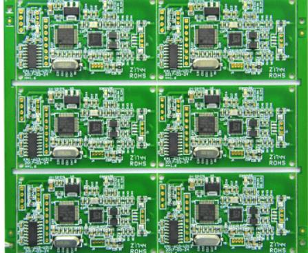
PCBA manufacturability
It does not meet the requirements of manufacturing capacity, which requires a lot of maintenance work, resulting in low product quality and multiple modifications of product design.
The products can not be manufactured at all, and designers must start from scratch, which wastes a lot of manpower and material resources and seriously weakens the competitiveness of enterprises in the same industry.
Poor product reliability, many customer complaints, large investment in after-sales service, the enterprise cannot make ends meet, and the product life cycle is shortened, which ultimately makes it difficult for the enterprise to sustain.
The manufacturability of PCBA is an important factor that must be considered in the design of modern electronic products. All kinds of problems are related to the manufacturability of PCBA.
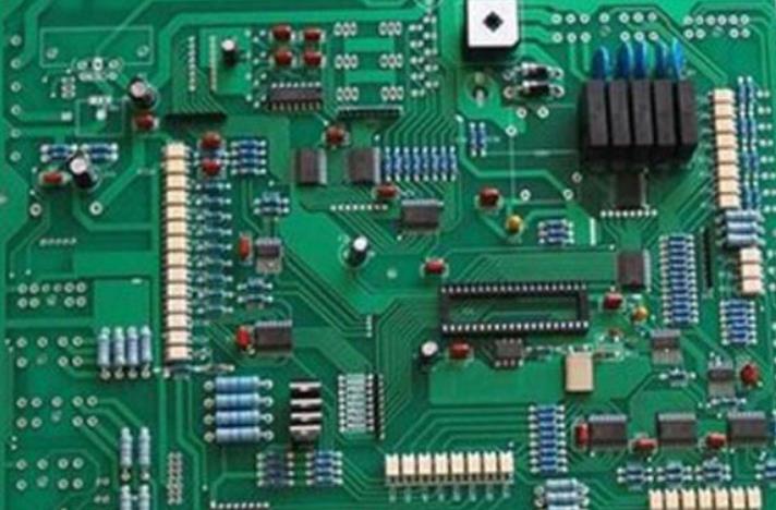
Guidelines for rework and repair (denso refurbishment, secondary bonding) in PCBA
Rework and repair of PCBA

Basis for rework and repair: There are no design files and regulations for rework and repair, no approval according to relevant regulations, and no specific regulations for rework and repair processes.
Number of rework allowed for each welding point: defective welding points are allowed to be reworked, and the number of rework allowed for each welding point shall not exceed 3 times, otherwise the weldment will be damaged.
Use of disassembled parts: In principle, disassembled parts shall not be used again. If it is necessary to use, it must be screened and tested according to the original power and technical performance of the components, and can be installed only after meeting the requirements.
Soldering off times on each pad: each printed pad can only be soldered off once (that is, only one component is allowed to be replaced). The thickness of intermetallic compound (IMC) of qualified solder joints is 1.5 3.5 µ m. After remelting, the thickness will increase, even reach 50 µ m. The solder joints become brittle, the welding strength decreases, and there is a serious reliability risk under vibration conditions; The remelting IMC requires a higher temperature, otherwise the IMC cannot be removed. The copper plating layer at the through hole outlet is the thinnest, and it is easy to disconnect the bonding pad from it after remelting; With the thermal expansion of Z-axis, the copper layer is deformed, and the solder pad is separated due to the obstruction of lead tin solder joints. In the case of lead-free, the entire pad will be pulled up: due to the moisture in the glass fiber and epoxy resin, the PCB will be layered after heating: the pad is easy to warp and separate from the substrate after multiple welding.
Bending and torsion requirements for surface mount and hybrid mount PCBA assembly and welding: bending and torsion requirements for surface mount and hybrid mount PCBA assembly welding are less than 0.75%
Total maintenance times of PCB assembly: The total maintenance times of a PCB assembly are limited to six, and excessive maintenance and modification will affect the reliability.
The above is the explanation given by the editor of pcb circuit board company.
If you want to know more about PCBA, you can go to our company's home page to learn about it.
In addition, our company also sells various circuit boards,
High frequency circuit board and SMT chip are waiting for your presence again.


Just upload Gerber files, BOM files and design files, and the KINGFORD team will provide a complete quotation within 24h.