
Professional PCB manufacturing and assembly
Building 6, Zone 3, Yuekang Road,Bao'an District, Shenzhen, China
+86-13410863085Mon.-Sat.08:00-20:00

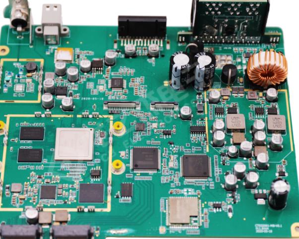
Manual visual inspection during PCBA processing
At present, manual visual inspection of PCB processing is mainly conducted by naked eyes or some relatively simple optical magnification instruments, PCB solder paste printing and manual visual inspection of solder joints. This is an effective method with less investment. For the process of manufacturers with low requirements and imperfect equipment and testing equipment, manual visual inspection plays an important role in improving the quality of assembly products
Manual visual inspection includes: manual inspection of PCB, manual visual inspection of glue point, manual visual inspection of solder joint, visual inspection of PCB surface quality, etc.
After the solder paste printing, component placement and welding are completed, manual visual inspection is required first. The main inspection contents are as follows:
(1) Solder paste printing. First, check whether the parameter settings of the solder paste printer are correct, whether the solder paste of PCB is printed on the bonding pad, whether the height of the solder paste is the same or "trapezoidal", but the edges of the solder paste should not be rounded or folded into a pile. When the steel plate is separated, it is allowed to pull up a small amount of solder paste to produce some peak shapes. If the solder paste is unevenly distributed, check whether the solder paste on the wiper plate is insufficient or unevenly distributed. It is necessary to check parameters such as printed steel plate. Finally, check whether the printed solder paste is bright under the microscope.
Circuit board

(2) Placement of components. Before placing the components on the first PCB with solder paste, please confirm whether the data rack is placed correctly, whether the components are correct, and whether the machine's picking position is correct before printing. After completing the first PCB, check in detail whether each component is correctly placed and gently pressed into the center of the solder paste, rather than just "placed" on the top of the solder paste. If you can see a slight dent in the solder paste in the microscope, it means it is placed correctly. Are all components in the bill of materials (BOM) consistent with those on the PCB, and are all components sensitive to positive and negative electrodes, such as diodes, tantalum electrolytic capacitors and integrated circuits, placed in the correct direction?
Why not use a clean process in SMT
SMT chip processing
1. The wastewater discharged after product cleaning in the production process pollutes the water quality, the earth and even animals and plants.
2. In addition to water cleaning, organic solvents containing hydrogen fluoride (CFC and HCFC) are also used for cleaning, which will also pollute and damage the air and atmosphere.
3. Detergent residues on the board will cause corrosion, which will seriously affect the product quality.
4. Reduce cleaning process operation and machine maintenance costs.
5. No cleaning can reduce the movement and cleaning during PCBA There are still some components that cannot be cleaned
6. The flux residue has been controlled and can be used according to the product appearance requirements to avoid visual inspection of the cleaning state.
7. The residual flux continuously improves its power efficiency to avoid leakage and any damage to the finished product.
8. The cleaning free process has passed many international safety tests, proving that the chemical substances in the flux are stable and non corrosive.


Just upload Gerber files, BOM files and design files, and the KINGFORD team will provide a complete quotation within 24h.