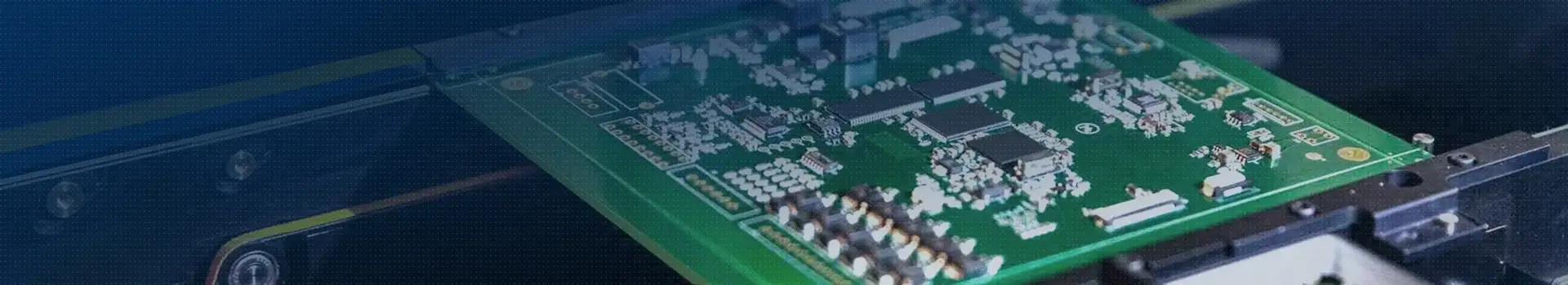
The etching process of PCB outer circuit was revealed
The more links there are, the more likely there will be problems. This can be regarded as a very spe...

The more links there are, the more likely there will be problems. This can be regarded as a very spe...
With the expansion of 5G commercial pace, the upgrading of consumer electronic products and the emer...
With the expansion of 5G commercial pace, the upgrading of consumer electronic products and the emer...
The shortest and widest printed line permitted by the assembly process shall be used. For high frequ...

Avoid running digital clock lines and high frequency analog signal lines near the power layer; other...

PCB customization, BOM, material selection and other electronic industry supply chain solutions, one...

Some customers have designed contour lines for Keep layer, Board layer, Top over layer and so on, an...
Correct PCB pad design, if there is a small amount of skew during patch processing, can be corrected...

The PCB of digital circuit can be composed of a wide ground wire circuit, that is, to form a ground ...
From the point of view of function, the hole can be divided into two categories: one is used as an e...
Vertical refers to the component body perpendicular to the circuit board installation, welding, its ...
There is no through hole between the welding pads of components without external pins (such as chip ...
