
Professional PCB manufacturing and assembly
Building 6, Zone 3, Yuekang Road,Bao'an District, Shenzhen, China
+86-13410863085Mon.-Sat.08:00-20:00


LG Group of Korea was founded in 1947 in Seoul, Korea, located at 20 Yeouido Dong, Yeongdeungpo-gu, Seoul. It is an international enterprise group leading the world's industrial development. [1] LG Group has established more than 300 overseas offices in 171 countries and regions. Its subsidiaries include LG Electronics, LG display, LG Chemicals, and LG Household & Health Care. Its business covers chemical energy, electronics, telecommunications, and services.
On November 28, BusinessKorea reported that LG Innotek will exit the HDI market and strategically shift labor and resources to the semiconductor business.
LG Innotek announced that it has decided to terminate its printed circuit board (PCB) business, which is part of the HDI business and accounted for 3.1 percent of the company's total sales. LG Innotek is expected to end PCB production within this year and stop selling PCBS in June next year.
LG Innotek explained that the business was suspended due to weakness in the HDI business due to declining demand for high value-added products from mobile devices and increased competition. Earlier, the company had said it was considering various plans, including exiting the HDI business to simplify its substrate business.
LG Innotek's PCB business sales depend on its sibling, especially smartphones, analysts said. This year, LG Innotek produced about 156,000 PCBS, less than 30 percent of its annual output between 2013 and 2016, and the plant's operating rate has fallen to about 51 percent.
LG Innotek said that after the closure of the PCB business, some resources will be transferred to its semiconductor substrate business, and its PCB staff will be deployed to the semiconductor substrate business.
"We want to improve our business portfolio by choosing and focusing on businesses that can grow and generate profits," an LG Innotek spokesman said.
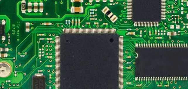
PCB layout is easy to be ignored in the 12 details
The spacing between patch components is a problem that engineers must pay attention to in layout. If the spacing is too small, it is very difficult to print solder paste and avoid soldering tin.

1. Distance suggestions are as follows
Device distance requirements between patches:
Same device: ≥0.3mm
Dissimilar devices: ≥0.13*h+0.3mm (h is the maximum height difference of nearby components)
The distance between components that can only be manually placed is required to be ≥1.5mm.
The above suggestions are for reference only and can be in accordance with the PCB process design specifications of the respective companies
2. Distance between in-line device and patch
A sufficient distance should be kept between the in-line resistance device and the patch. It is recommended that the distance should be between 1-3mm. Due to the trouble of processing, there are few cases of using the in-line plug-in.
3, for the IC decoupling capacitor placement
The decoupling capacitor must be placed near the power port of each IC as close as possible to the IC power port. If a chip has multiple power ports, the decoupling capacitor must be placed at each port.
4. Attention should be paid to the direction and distance of components placed on the edge of PCB board
Since PCBS are generally made with a patchwork board, the device near the edge needs to meet two conditions. The first is parallel to the cutting direction. (Make the mechanical stress of the device even. For example, if the device is placed according to the way on the left of the figure above, the different stress directions of the two pads when the plate is to be split may lead to the loss of the element and the pad). The second is that devices cannot be placed within a certain distance. (Prevent the board from damaging components when cutting)
Bioneng belongs to Qinji Group, is the leading electronic industry service platform in China, providing online components, sensor procurement, PCB customization, BOM, material selection and other electronic industry supply chain solutions, one-stop to meet the comprehensive needs of small and medium-sized customers in the electronics industry.
5. Attention should be paid to the fact that adjacent pads need to be connected
If the adjacent pad needs to be connected, first confirm the connection on the outside to prevent the bridge caused by a ball, and pay attention to the width of the copper wire at this time.
6, if the pad falls in the ordinary area need to consider heat dissipation
If the pad falls in the paving area, the right way should be adopted to connect the pad to the paving, and determine whether to connect 1 wire or 4 wires according to the size of the current. If the left way is adopted, it is more difficult to weld or repair and disassemble components, because the temperature is fully dispersed through the copper paving, resulting in the welding of the fish.
7. If the lead is smaller than the plug-in pad, you need to add tears
If the wire is smaller than the pad of the in-line device, you need to add a tear drop in the way shown on the right.
Adding teardrops has the following benefits:
1. Avoid reflection caused by sudden reduction of signal wire width, which can make the connection between wire and component pad smooth transition.
2. Solve the problem that the connection between the pad and the wire is easy to break under the impact force.
3, set the tear drop can also make the PCB board appear more beautiful.
8. The lead width on both sides of the component pad should be consistent
9. Pay attention to keep the pad without using pins, and ground it correctly.
If two pins of a chip do not use the situation, but the chip physical pins are there, if the two pins are in a state of suspension is easy to cause interference. Interference can be avoided by adding a pad and grounding the pad.
10, pay attention to the best through hole not on the pad, easy to cause tin leakage welding.
11. Pay attention to the distance between wires or components and the edge of the plate
Note that the lead or components can not be too close to the edge of the plate, especially the single panel, the general single panel is mostly paper board, easy to break after the force, if in the edge line or put components will be affected.
12, must consider the environmental temperature of the electrolytic capacitor away from the heat source
Firstly, whether the ambient temperature of the electrolytic capacitor meets the requirements should be considered. Secondly, the capacitor should be kept away from the heating area as far as possible to prevent the liquid electrolyte inside the electrolytic capacitor from being dried.


Just upload Gerber files, BOM files and design files, and the KINGFORD team will provide a complete quotation within 24h.