
Professional PCB manufacturing and assembly
Building 6, Zone 3, Yuekang Road,Bao'an District, Shenzhen, China
+86-13410863085Mon.-Sat.08:00-20:00


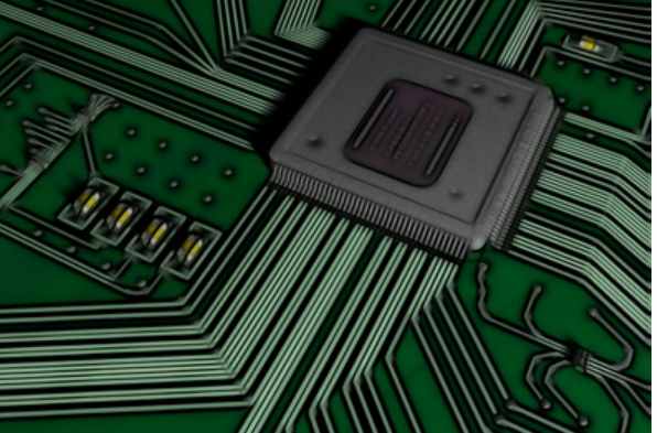
PCB wiringis very important in the whole pcb design, how to do fast and efficient wiring, and let your PCB wiring look tall, is worth studying. Sorted out the PCB wiring needs to pay attention to 7 aspects, quick to check the gaps!
1. Common ground processing of digital circuit and analog circuit
There are now many PCBS that are no longer single-function circuits (digital or analog), but consist of a mix of digital and analog circuits. Therefore, it is necessary to consider the interference between them when wiring, especially the noise interference on the ground wire. The digital circuit has a high frequency and the analog circuit has a strong sensitivity. For the signal line, the high frequency signal line is far away from the sensitive analog circuit devices as far as possible. For the ground wire, the rectifier PCB has only one node to the outside world, so the problem of number and mode common ground must be handled inside the PCB, and the digital and analog ground are actually separated from each other in the board. Only at the interface (such as plug, etc.) between PCB and the outside world. There is a little bit of short circuiting between digital and analog, but note that there is only one connection point. There are also differences on the PCB, which is determined by the system design.

2. The signal cable is distributed on the electrical (ground) layer
In the multi-layer printed board wiring, because in the signal line layer is not finished the line is not much, and then more layers will cause waste will also increase the production of a certain amount of work, the cost is increased accordingly, in order to solve this contradiction, you can consider wiring on the electrical (ground) layer. The power layer should be considered first and the formation second. Because it's better to preserve the integrity of the formation. Bioneng belongs to Qinji Group, is the leading electronic industry service platform in China, providing online components, sensor procurement, PCB customization, BOM, material selection and other electronic industry supply chain solutions, one-stop to meet the comprehensive needs of small and medium-sized customers in the electronics industry.
3. Processing of power supply and ground wire
Even if the wiring in the whole PCB board is completed very well, but because of the power supply, ground wire is not thoughtful and caused by interference, will make the performance of the product decline, sometimes even affect the success rate of the product. So the wiring of the power supply and ground wire should be taken seriously, the noise interference generated by the power supply and ground wire should be reduced to a minimum to ensure the quality of the product. For every engineering personnel engaged in the design of electronic products will understand the cause of the noise between the ground and the power line, now only to reduce the noise suppression is described: it is well known that between the power supply and the ground to add the coupling capacitance. Try to widen the width of the power supply, ground wire, it is best that the ground wire is wider than the power line, their relationship is: ground wire > Power cord > Signal cable, usually signal cable width: 0.2 ~ 0.3mm, the maximum fine width can be up to 0.05 ~ 0.07mm, power cable is 1.2 ~ 2.5 mm. The PCB of digital circuit can be composed of a wide ground wire circuit, that is, to form a ground network to use (the ground of analog circuit can not be used in this way) with a large area of copper layer as ground, in the printed board is not used to connect with the ground as ground. Or made of multilayer board, power supply, ground wire each occupy a layer.
4. The role of network system in wiring
In many CAD systems, the wiring is determined by the network system. Although the grid is too dense, the path is increased, but the step is too small, the amount of data in the graph field is too large, which inevitably has higher requirements for the storage space of the equipment, but also has a great impact on the computing speed of the object computer electronic products. Some paths are invalid, such as those occupied by the pad of the component leg or those occupied by the mounting holes and fixing holes. Too sparse grid and too few channels have great influence on the propagation rate. So there should be a reasonable grid system to support the wiring. The distance between the legs of a standard component is 0.1 inch (2.54mm), so grid systems are generally based on 0.1 inch (2.54mm) or integral multiples less than 0.1 inch, such as 0.05 inch, 0.025 inch, 0.02 inch, etc.
5. Processing of connecting legs in large area conductors
In a large area of grounding (electricity), the legs of commonly used components are connected to it, and the treatment of the connecting legs needs comprehensive consideration. In terms of electrical performance, the welding pad of the legs of components is fully connected with the copper surface, but there are some bad risks for the welding assembly of components, such as: ① welding requires a high-power heater. (2) easy to cause virtual solder joints. Therefore, taking into account the electrical performance and process needs, make a cross welding pad, called heat shield, commonly known as Thermal pad (Thermal), so that when welding due to excessive heat dissipation section and the possibility of virtual solder joint greatly reduced. The electrical connection (ground) leg of the multilayer plate is treated the same.
PCB mixed signal circuit board design criteria
Apr 16,2023


Just upload Gerber files, BOM files and design files, and the KINGFORD team will provide a complete quotation within 24h.