
Professional PCB manufacturing and assembly
Building 6, Zone 3, Yuekang Road,Bao'an District, Shenzhen, China
+86-13410863085Mon.-Sat.08:00-20:00

Shape and simplify the production process. Due to its strong ability to withstand high currents, the 3.3V power layer and the corresponding grounding layer should be coated with 1 oz copper, and the other layers can be coated with 0.5 oz copper. This reduces voltage fluctuations caused by transient high currents or spikes.
If you are designing a complex system from the ground up, use 0.093 inch and 0.100 inch thick cards to support the wiring layer and grounding isolation layer. The thickness of the card must also be adjusted according to the wiring characteristics of the perforated plate and the hole so that the aspect ratio of the hole diameter to the finished card thickness does not exceed the aspect ratio of the metallized hole provided by the manufacturer.
If a low-cost, high-yield commercial product is to be designed with a minimum number of wiring layers, carefully consider the wiring details of all special power supplies on a mixed-signal PCB before laying out or wiring. Have the target manufacturer review the preliminary layering scheme before starting the layout and wiring. Layering is basically based on the thickness of the finished product, the number of layers, the weight of the copper, the impedance (with tolerance) and the minimum size of the through hole pads and holes. The manufacturer should provide layering recommendations in writing.

Examples of configurations of all controlled impedance strip and microstrip lines should be included in the recommendation. Your impedance predictions are considered in conjunction with the manufacturer's impedance predictions, which can then be used to verify signal wiring characteristics in the simulation tools used to develop CAD wiring rules.
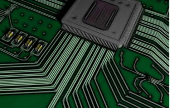
The layout of OC48 card
The high speed analog signal between the optical transceiver and the DSP is very sensitive to external noise. Similarly, all the special power and reference voltage circuits also create a lot of coupling between the card's analog and digital power transmission circuits. Sometimes, due to the limitations of the housing shape, high-density board cards have to be designed. Due to the orientation of the external optical cable access card and the high size of some components of the transceiver, the position of the transceiver in the card is fixed to a large extent. The system I/O connector position and signal allocation are also fixed. This is the groundwork that must be done before the layout.
As with most successful high-density analog layout and wiring schemes, the layout needs to meet the wiring requirements, and the layout and wiring requirements must be mutually compatible. For the analog part of a mixed-signal PCB and the local CPU core with 2V operating voltage, the "layout before wiring" method is not recommended. For OC48 cards, the part of the DSP analog circuit that contains the analog reference voltage and the analog power supply bypass capacitor should be wired interactively first. After the wiring is completed, the entire DSP with analog components and wiring should be placed close enough to the optical transceiver to fully ensure the shortest wiring length, minimum bending and minimum holes for high-speed analog differential signals to the DSP. The symmetry of the differential layout and wiring will reduce the effect of common-mode noise. However, it is difficult to predict the best layout before wiring.
Consult your chip distributor for PCB board design guidelines. Fully communicate with the distributor's application engineer before designing according to the guidelines. Many chip distributors have strict time limits for providing high-quality cloth recommendations. Sometimes, the solution they provide is feasible for a "Tier 1 customer" using the device. In the field of signal integrity (SI) design, the signal integrity design of new devices is particularly important. Following the distributor's basic guidelines and in conjunction with the specific requirements for each power and ground pin in the package, you can begin wiring the OC48 card with DSP and microprocessor integrated.
After the location and wiring of the high-frequency analog part is determined, the rest of the digital circuit can be placed according to the grouping method shown in the block diagram. Care should be taken to carefully design the following circuits: the location of the PLL power filter circuit in the CPU that is sensitive to analog signals; Local CPU kernel voltage regulator; A reference voltage circuit for "digital" microprocessors.
Electrical and manufacturing specifications for digital wiring can then be properly applied to the design. The aforementioned design of signal integrity for high-speed digital buses and clock signals reveals some special wiring topology requirements for processor buses, balanced Ts, and time-delay matching for some clock signal wiring. But what you may not know is that someone else has proposed an update, which is to add several terminal resistors.
In the process of solving the problem, it is natural to make some adjustments in the layout stage. However, before you begin wiring, it is important to verify the timing of the digital sections against the layout scheme. At this point, a full DFM/DFT layout review of the board will help ensure that the card meets the customer's needs.
Digital wiring for OC48 cards
For the power lines of digital devices and the digital parts of mixed-signal DSPS, the digital wiring starts with SMD escape patterns. The shortest and widest printed line permitted by the assembly process shall be used. For high frequency devices, the printed line of the power supply is equivalent to a small inductance, which will worsen the power supply noise and cause undesired coupling between the analog and digital circuits. The longer the power supply print line, the greater the inductance.
The optimal layout and wiring scheme can be obtained by using digital bypass capacitor. In short, the position of the bypass capacitor is fine-tuned as needed to make it easy to install and distribute around the digital parts of digital components and mixed-signal devices. The same "shortest and widest route" method is used to route the bypass capacitance outlet diagram.
summarize
After the completion of OC48 cable board, the signal integrity check and timing simulation should be carried out. Simulation results show that the wiring instruction meets the expected requirements and improves the timing index of the second layer bus. The final design rule check, final manufacturing review, light mask and review and issued to the manufacturer, then the board layout task is officially completed.

Maintenance of pcb etching equipment
Apr 16,2023


Just upload Gerber files, BOM files and design files, and the KINGFORD team will provide a complete quotation within 24h.