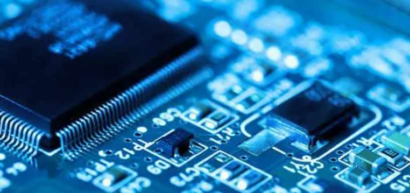
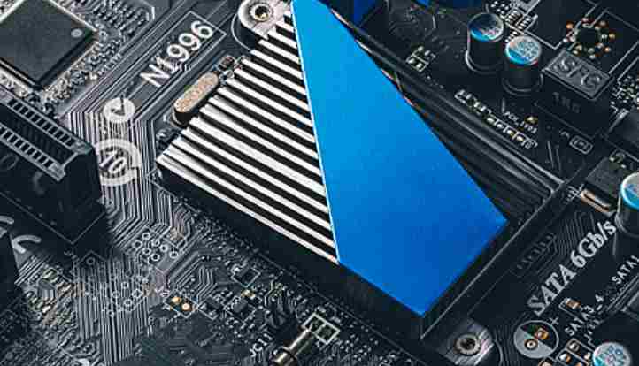
How to reduce ESD interference in PCB design process
in the design of PCB board, PCB anti-ESD design can be realized by layering, proper layout and wirin...


in the design of PCB board, PCB anti-ESD design can be realized by layering, proper layout and wirin...
Aluminum substrate and FR4 board are two common PCB board, aluminum substrate is commonly used as LE...
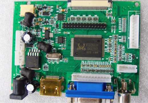
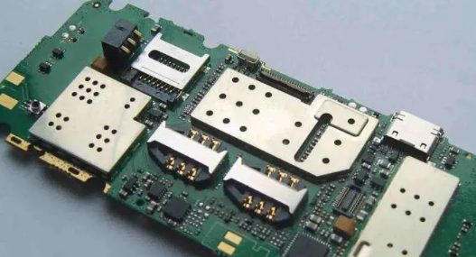
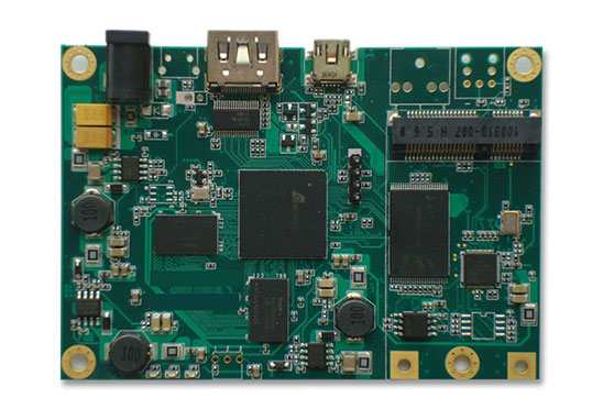
PCBA machining circuit board debugging steps and methods: 1. Board surface observation and resistanc...
Circuit board PCBA processing process can be roughly divided into: empty plate loading - printed sol...
Pay attention to the wiring of signal lines under the magnetic beads, between the pads and those tha...
Ensure the machining accuracy and assembly accuracy of guide column and guide sleeve; Reduce the fit...
Four proofing methods of aluminum substrate: one, photographic material proofing method, two, mechan...
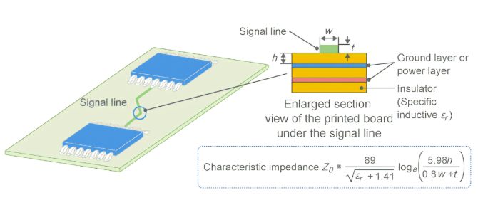
Only under certain conditions can the 20H principle have obvious effects. 1. The power plane shall b...
Common bad reasons for PCBA welding resistance film processing :1. Welding pad and through hole conn...
The difference between them is that the core is thinner, the pp sheets of one or two layers and five...
The characteristics of the gold process: the copper on the circuit board is mainly copper, copper so...
The function of PCB design discharge teeth: in surge testing or ESD testing, the two ends of the com...
