
Professional PCB manufacturing and assembly
Building 6, Zone 3, Yuekang Road,Bao'an District, Shenzhen, China
+86-13410863085Mon.-Sat.08:00-20:00

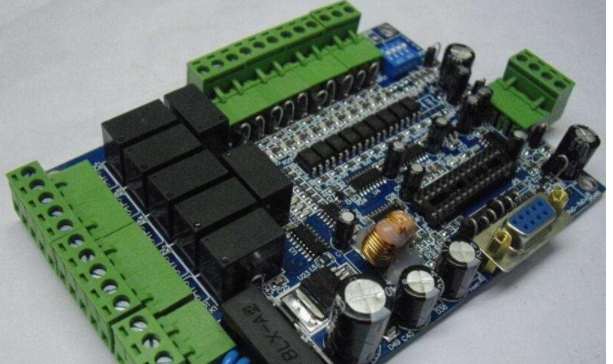
After PCBA processing is completed, it is necessary to debug the circuit board to verify whether its function meets the design requirements. This is a set of system engineering. Next, Shenzhen PCBA processing manufacturer -kingford will introduce the debugging steps and methods of PCBA processing circuit board.
The debugging procedure and method of PCBA machining circuit board
1. Board surface observation and resistance check
First of all, we should roughly observe whether there are problems on the board, such as whether there are cracks, short circuit, open circuit and other phenomena. If necessary, check that the resistance between the power supply and the ground wire is large enough.
2. Install components
Independent modules, in the absence of a guarantee that they work normally, it is best not to install all, but part by part, so that it is easy to determine the scope of PCB fault.
3. Check the output voltage of the power supply
Generally speaking, you can install the power supply part first, and then power on to test whether the output voltage of the power supply is normal. During power-on, you can consider using an adjustable voltage regulator with current limiting function.
4. Preset overcurrent protection current
Firstly, the over-current protection current is preset, and then the voltage value of the regulated power supply is gradually increased, and the input current, input voltage and output voltage are monitored. If there are no current protection problems during the up-regulation process, and the output voltage also reaches normal, it indicates that the power supply is partially normal.
5. Install other modules and power on them
Gradually install other modules. After each module is installed, power it on to test it to avoid burning out components due to overcurrent caused by design errors or component installation errors.

2. High Speed PCB Design Ten Tips for PCB Laminated design
With the emergence of high-speed circuits, the complexity of PCB board is becoming higher and higher. In order to avoid the interference of electrical factors, the signal layer and the power layer must be separated, so it involves the design of multi-layer PCB, namely the design of laminated structure.
Good lamination design can not only effectively improve the quality of power supply, reduce crosstalk and EMI, improve signal transmission performance, but also save costs and provide convenience for PCB design and wiring, which is the first consideration of any high-speed PCB designer.
Ten Tips for PCB Layering Design
Step 1 Layer
A multilayer PCB usually contains a signal layer (S), a power supply (P) plane and a ground (GND) plane. The power plane and the ground plane are usually undivided solid planes that will provide a good low-impedance current return path for the current of adjacent signal routes. Most of the signal layers are located between these power or ground reference plane layers, forming symmetrical or asymmetric strip lines. The top and bottom layers of multilayer PCBS are usually used for placing components and a small amount of wiring. These signal wiring requirements should not be too long to reduce the direct radiation generated by the wiring.
2. Determine the reference plane of a single power supply (power plane)
The use of decoupling capacitors is an important measure to solve the integrity of power supply. Decoupling capacitors can only be placed on the top and bottom layers of the PCB. The routing, pad and hole of the decoupling capacitor will seriously affect the effect of the decoupling capacitor, which requires that the design must consider the connection of the decoupling capacitor should be as short and wide as possible, and the wire connected to the hole should also be as short as possible. For example, in a high-speed digital circuit, decoupling capacitors can be placed on the top layer of the PCB, layer 2 assigned to the high-speed digital circuit (such as the processor) as the power layer, layer 3 as the signal layer, and layer 4 as the high-speed digital circuit ground.
In addition, it is necessary to ensure that the signal routing driven by the same high-speed digital device takes the same power layer as the reference plane, and this power layer is the power supply layer of the high-speed digital device.
3. Determine the multiple power supply reference planes
The multiple power reference planes will be divided into several solid regions with different voltages. If the signal layer is close to the multi-power layer, the signal current in the signal layer near it will encounter an unsatisfactory return path, resulting in gaps in the return path. For high-speed digital signals, this unreasonable return path design may cause serious problems, so it is required that high-speed digital signal PCB design wiring should be far away from the multi-power reference plane.
4. Determine multiple ground reference planes (ground planes)
Multiple ground reference planes (grounding planes) provide a good low-impedance current return path that reduces common-mode EMl. The ground plane and the power plane should be tightly coupled, and the signal layer should also be tightly coupled to the adjacent reference plane. This can be achieved by reducing the thickness of the medium between layers.
5. High-speed signal layer is located in the middle layer of signal
The high-speed signal transmission layer in the circuit should be the signal intermediate layer, and sandwiched between two copper-coated layers. In this way, the two coppered copper films can provide electromagnetic shielding for high-speed signal transmission, but also effectively limit the radiation of high-speed signals between the two coppered layers, without causing external interference.
6. Set the PCB design and wiring direction
In the same signal layer, the direction of most PCB design wiring should be ensured to be consistent, and at the same time should be orthogonal to the direction of PCB design wiring in adjacent signal layers. For example, the PCB design wiring direction of one signal layer can be set as the "Y-axis" strike, while the PCB design wiring direction of another adjacent signal layer can be set as the "X-axis" strike.
7. Keep the multiple power layers away from the high-speed signal layer
Multiple power layers should be careful away from high speed digital signal PCB design wiring. Because the multiple power layers are divided into several solid areas with different voltages, if the signal layer is close to the multiple power layers, the signal current on the nearby signal layer will encounter an unsatisfactory return path, resulting in gaps in the return path.
8. Use an even layer structure
Classic PCB lamination designs are almost entirely even layers, rather than odd layers. Even layers of printed circuit boards have cost advantages, and even layers can avoid board warping more than odd layers.
9. PCB design and wiring combinations are arranged in adjacent layers to complete complex PCB design and wiring
Switching between layers is inevitable. The two layers that a signal path crosses are called a "PCB design wiring assembly". The best PCB design wiring combination design is to avoid the flow of return current from one reference plane to another reference plane, but from one point (face) of one reference plane to another point (face). Therefore, PCB design wiring combinations are best arranged in adjacent layers, because a path through multiple layers is not unobstructed for return current. Although the ground elastic can be reduced by placing decoupling capacitors near the holes or reducing the thickness of the medium between the reference planes, it is not a good design.
10. Cost consideration
In terms of manufacturing cost, with the same PCB area, the cost of multilayer boards is definitely higher than that of single and double layer boards, and the more layers, the higher the cost. However, when considering the realization of circuit function and circuit board miniaturization, ensuring signal integrity, EMl, EMC and other performance indicators, multi-layer circuit board should be used as far as possible. Overall evaluation, the cost difference between multilayer circuit board and single and double layer circuit board is not much higher than expected.
kingfordPCBA processing capability
1. Maximum board card: 310mm*410mm(SMT);
2. Maximum plate thickness: 3mm;
3. Minimum plate thickness: 0.5mm;
4. Minimum Chip parts: 0201 package or parts above 0.6mm*0.3mm;
5. Maximum weight of mounted parts: 150g;
6. Maximum parts height: 25mm;
7. Maximum parts size: 150mm*150mm;
8. Minimum spacing of pin parts: 0.3mm;
9. Minimum ball parts (BGA) spacing: 0.3mm;
10. Minimum ball parts (BGA) ball diameter: 0.3mm;
11. Maximum parts mounting accuracy (100QFP) : 25um@IPC;
12. Patch capacity: 3-4 million points/day.
kingford specializes in providing overall PCBA electronic manufacturing services, including upstream electronic component procurement to PCB production and processing, SMT patches, DIP plug-ins, PCBA testing, finished product assembly and other one-stop services.


Just upload Gerber files, BOM files and design files, and the KINGFORD team will provide a complete quotation within 24h.