
Professional PCB manufacturing and assembly
Building 6, Zone 3, Yuekang Road,Bao'an District, Shenzhen, China
+86-13410863085Mon.-Sat.08:00-20:00

When you are doing PCB design, you need to choose the laminated scheme of our board. A good laminated scheme can make our signal quality better, and the performance of the board will be more stable, etc. You may have more or less contact with the multilayer board, that is, the board with two layers up, so you have heard of the "false eight layers" when you are doing the six-layer board. What does "false eight floors" mean? Is he six stories or eight? Before we can figure this out, we need to understand the following two points.
First, PCB laminated knowledge
Our PCB board is usually composed of core board, copper foil, semi-cured sheet (also known as PP sheet) and solder resistance oil.
Core board: It is composed of copper foil, solid resin material and glass fiber, which is the basic material for making PCB. It has certain hardness and thickness, and both surface layers have copper foil.
Semi-cured sheet (PP sheet) : mainly composed of resin and reinforcing material, reinforcing material is divided into glass fiber cloth, paper base, composite material and other types, and the production of multi-layer printed board used in the semi-cured sheet (bond sheet) is mostly made of glass fiber cloth as reinforcing material.

Two, PCB impedance basic knowledge
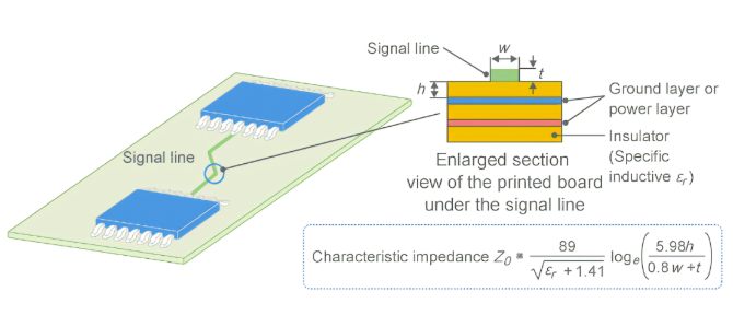
Now that we have a brief look at the composition of our board, there is one more thing we need to know, and that is impedance. With the rapid improvement of signal transmission speed and the wide application of high frequency circuit, higher requirements are put forward for printed circuit boards. The circuit performance provided by the printed circuit board must be able to make the signal in the transmission process without reflection phenomenon, signal integrity, reduce transmission loss, play the role of matching impedance, so as to get a complete, reliable, accurate, no interference, noise transmission signal. Impedance matching is very important in high frequency design. Impedance matching is related to signal quality. The main purpose of impedance matching is that all high-frequency microwave signals on the transmission line can reach the load point, and no signal will be reflected back to the source point.

Usually the factors that affect our impedance are mainly plate, dielectric constant, copper thickness, solder resistance oil, line width and so on. If it is a difference line, then the distance between the difference lines will also affect the impedance. General medium thickness, the distance between the difference line and the impedance is proportional to the copper thickness, line width and impedance is inversely proportional to the general welding resistance brush up will also reduce our impedance value.
Impedance basics of PCB
Three, after we know these knowledge, we can enter the topic, what is the "false eight layers" :
As shown in the figure above, there are two core boards inside. The thickness of pp sheets of the first and fifth layers is 6.68mil, and the thickness of core sheet is 9.84mil. There are three pp sheets between the core board and the core board, so the thickness reaches 20.92mil. If we have a lot of impedance lines on the board at this time, we will find through calculation that the bottom of the table needs to control 50om single end of the line width is 11mil, 100om difference line width and line distance is 8.5mil/9mil, and the inner layer of 50om single end line width reached 12.50mil, The difference line width is 6.8mil/8mil,
The small width of the line undoubtedly increases the difficulty of our design, and it may even be impossible to design it. Therefore, we can reduce the width of the line and meet the requirements of impedance by changing the method of stacking. From the impedance knowledge introduced above, we know that the thickness of the medium is proportional to the impedance value. Therefore, if we want to reduce the line width of the surface layer, we can reduce the thickness of the medium by reducing the number of pp sheets between the surface layer and the second layer and choosing thinner pp sheets. At this time, when the thickness of the medium decreases, the impedance value will be smaller, so we can reduce the line width to achieve our target impedance value. Due to the symmetry of the layers, the line width of the bottom layer is also reduced by this method.
The third layer refers to the second layer and the fifth layer, among which the third layer is close to the second layer GND plane and the fifth layer is far away from the third layer. We mainly refer to the second layer GND plane, which is more influenced by the second layer. Therefore, we can reduce the value of core by changing the type of core board, and the thickness of medium is reduced. In the case of the same line width of the third layer, the smaller the impedance value, then we need to achieve the target impedance value is the same. It is OK to reduce the line width, so that the inner layer also reduces the line width and meets the requirements of impedance. The fourth layer is also the same, but at this time, we will find that the pp sheet between the first and second layers and the fifth and sixth layers is thinner, and the core plate is thinner. At this time, to achieve the target plate thickness, we can only increase the thickness between the core plate and the core plate. We can increase the number of pp sheets to achieve the purpose of thickening, but we cannot increase the number of pp sheets all the time. Generally, only three pp sheets can be used at most. We have introduced the composition of the core board and pp sheet above, which both contain resin and glass fiber, but there is a copper foil on both sides of the core board. We can add a "core board" between the core board and the core board to meet our plate thickness requirements, but we have removed the copper foil on both sides of this "core board". The new stack is shown below

At this time, we find that the 50om single terminal line width at the bottom of the table is 5.7mil, the 100om differential line width is 4.1mil/8.2mil, and the inner 50om impedance single terminal line width is 5.3mil, and the 100om differential distance is 4.1mil/8.2mil
This line width is generally acceptable for conventional design, so we can compare the two layers, and you will find that the difference between them is that the core is thinner, and the pp sheets of the first and second layers and the fifth and sixth layers are also thinner. There is a core board without copper foil on both sides between the core PCB boardand the core board, so generally this kind of layer is called "false eight layers".
Four, after understanding the differences between them, we can also sum up their advantages and disadvantages:
1, in the case of impedance, we use the design of false eight layers can reduce our design line width, so as to meet our design requirements.
2, in the case of six-layer laminated third layer and fourth layer of the use of false eight-layer design can reduce the crosstalk between the third layer and the fourth layer, because the third layer and the fourth layer are adjacent layers, to go the line, the two layers are too thin between the case will produce crosstalk, affecting the quality of the signal, so we increase the distance between the two layers of the design of false eight-layer, Crosstalk will be relatively small, but we also need to note that, in the case of adjacent wiring layers, we should use "vertical wiring", that is, one layer goes horizontal, the other layer goes vertical.
3. Due to the increase of materials, our cost will also increase accordingly. Fake eight layers is more expensive than six layers, but cheaper than eight layers.


Just upload Gerber files, BOM files and design files, and the KINGFORD team will provide a complete quotation within 24h.