
Professional PCB manufacturing and assembly
Building 6, Zone 3, Yuekang Road,Bao'an District, Shenzhen, China
+86-13410863085Mon.-Sat.08:00-20:00

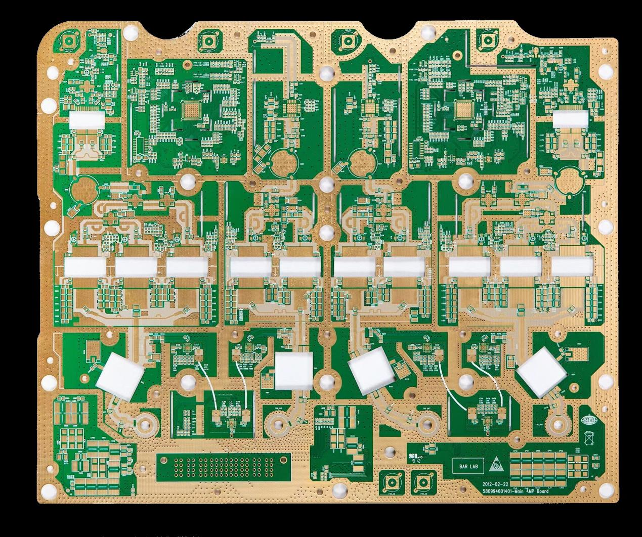
Since the development of circuit boards, many types have been derived, but most of them can be divided into two types: rigid and flexible PCB, and today we will talk about the structural composition of flexible PCB. Generally, circuit boards are divided into layers according to the number and thickness of conductive copper foils. They can be divided into single-layer boards, double-layer boards, multi-layer boards and double-sided boards. Their structures are also different. Where are their different properties.

Structure of single-layer board: This is the simplest flexible board structure, usually a set of raw materials bought by base material + transparent glue + copper foil, while protective film + transparent glue is another purchased raw material; first of all, copper The foil needs to be etched and other processes to obtain the required circuit, the protective film needs to be drilled to expose the corresponding pads, and after cleaning, the two are combined by rolling method, and then the exposed pads are plated with gold or Tin, etc. are used for protection, so that the large board is ready, and then it needs to be punched into a small circuit board of the corresponding shape.
Structure of double-layer board: When the circuit is too complicated, the single-layer board cannot be wired, or copper foil is required for grounding shielding, it is necessary to use a double-layer board or a multi-layer board. Structure of multi-layer board: The most typical difference between multi-layer board and single-layer board is the addition of via structure to connect each layer of copper foil. Generally, the first processing process of substrate + transparent glue + copper foil is to make via holes; First, drill holes on the substrate and copper foil, and then plated with a certain thickness of copper after cleaning, so that the vias are completed, and the subsequent production process is almost the same as that of the single-layer board.
Double-sided structure: There are pads on both sides of the double-sided board, which are mainly used for connection with other circuit boards. Although it is similar in structure to a single-layer board, the production process is very different. Its raw materials are copper foil, protective film + transparent glue. First, drill holes on the protective film according to the requirements of the pad position, and then paste the copper foil. Then corrode the pads and leads, and then paste another protective film with a drilled hole. Although these types of structures of flexible PCB are different, many manufacturing processes have the same characteristics, but different processes are added in some basic places to correspond to different fields.
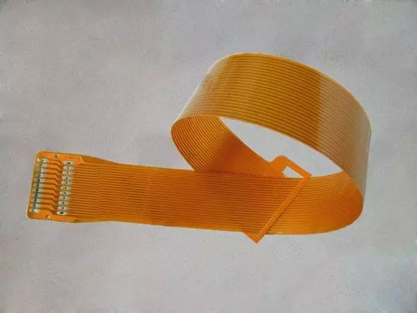
The development trend of miniaturization and multi-functionalization of electronic products will definitely promote the development of PCB manufacturing technology in the direction of high density, high precision, miniaturization and high speed. Since flexible PCB rely on substrate materials that are flexible and able to bend, which results in their light weight and small size,flexible PCB have witnessed their increasing application in electronic products in recent years. The development of PCB boards is closely related to the development of materials and technologies, so this article will discuss the development opportunities and challenges that flexible PCB must face in terms of new materials and technologies.
Innovation in flexible PCB largely depends on the growth of new materials. Material innovations in insulating substrate materials, adhesives, foils, overlays, and reinforcement boards are driving higher performance from circuit boards. Since flexible PCB manufacturing requires higher requirements for various materials, a diverse material system will provide manufacturers with a variety of options and combinations. Since flexible PCB technology utilizes flexible substrate materials, it is compatible and complementary to the popular printed electronics technology in recent years. Therefore, how to use printing technology to manufacture circuit boards in the additive process is a new topic that the flexible PCB industry should pay attention to.
Advances in materials and technology can further expand the application range of flexible PCB. For example, LED PCBs play a dominant role in the current market, depending on the design of rigid boards plus metal backplanes. With the optimization of heat resistance of materials,flexible PCB will be applied to thin and light LED products. Another notable application for flexible PCB is automotive PCBs. Until now, automotive electrical components have mostly utilized wire connections, and the equivalent thin flexible PCB is 70% lighter than wire. The breakthrough in the development of high polymer materials has improved the high temperature stable operating range from current 100°C to 125°C to 200°C or higher. In addition to high efficiency, excellent electrical sensing and control performance,flexible PCB will find more applications in automobiles and play a key role.
In the PCB industry, new materials and technologies often help each other, and they work perfectly on flexible PCB due to their higher demands on performance. During the fabrication of microvias in flexible PCB, the mechanical strength and deformation coefficients of different materials on different layers should be carefully considered, and the deformation should be estimated based on the results of through-hole fabrication. In the end, precise micropores will be successfully fabricated. With opportunity, all application expectations will present extreme challenges in PCB materials, technology and design. Therefore, when we want to go further in the PCB industry, adhering to technological innovation and independent research and development is an essential principle.


Just upload Gerber files, BOM files and design files, and the KINGFORD team will provide a complete quotation within 24h.