
Professional PCB manufacturing and assembly
Building 6, Zone 3, Yuekang Road,Bao'an District, Shenzhen, China
+86-13410863085Mon.-Sat.08:00-20:00

How to prevent solder bridging during PCBA production and operation
The term "bridge" is often synonymous with a previously unreachable area of connection or crossing. In wireless communications, the term bridging is applied to providing Internet connectivity between two wired networks via a Wi-Fi connection. In this case, the bridge (wireless) acts as a client by logging into the router and providing an Internet connection that is shared with the connected device.") https://www.kingfordpcb.com/yuan.php
https://www.kingfordpcb.com/yuan.php
However, in conjunction with welding, the term bridge has a completely different meaning in the following areas: printed circuit boards. Welding bridge is an error that can occur during welding. This is an issue that can affect manufacturing, have to be reworked, and cause unstable field operations. Understanding how to prevent solder bridging is a problem to be solved in optimizing circuit board manufacturing and operation. So let's delve into the causes of solder bridging and suggest ways to avoid it.
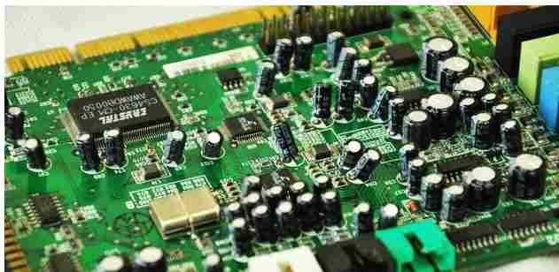
The continued focus on miniaturization of almost all electronic devices has led to increasing design requirements to fit more components into smaller and smaller package sizes. Miniaturization in particular presents various manufacturing problems, especially solder bridging.
Many problems can affect the welding process and lead to defects during board assembly. Solder bridging is a defect that occurs when two or more pads form a connection through excessive application of solder. Other welding problems (such as tombstones) are easier to identify, but without detailed instructions, solder bridging may not show up on optical inspection.
Undiagnosed problems such as solder Bridges can cause wiring damage, component damage or even short circuits. Since this is a critical issue, solder mask can prevent excessive solder application. A solder shield is a solderproof coating that is added to your PCB during manufacturing to protect certain areas of the PCB from the application of solder.
During the manufacturing process, various conditions can and will cause solder bridging. Welding Bridges can come from manufacturing equipment in use or even decisions made during the design process. Here are some of the more common reasons for solder bridging:
Incorrect formwork specifications can result in too much solder on the pad, resulting in surface mount technology (SMT).
During the printing process, a poor seal between the template and the bare plate can result in solder bridging.
Smaller pin spacing can result in a lack of sufficient clearance between the component pads, or no solder stop layer.
Incorrect or inaccurate assembly placement or assembly reduction can result in pad size correlation.
Setting the reflow furnace determines the temperature at which the solder wets and sets. CM Several precautions can be taken to avoid solder bridging problems. The following list describes the application areas.
A solder stop layer embossed is an area of the PCB layout that does not require a solder stop layer. We usually specify them as thin Outlines around through-hole pads, surface-mount pads, through-holes and test points.
In addition, solder resistance layers are subject to industry standards (IPC-SM-840D), which include shelf life, physical requirements, materials, etc.
A solder barrier dam acts as a barrier between applying solder to each pad. Make sure to provide a solder shield dam between each SMT pad. In essence, it acts as an actual (physical) dam.
As a recommendation, there should be a solder mask between each pad on the SMT assembly. This becomes more and more necessary as your PCBA (i.e. integrated circuit (IC)) becomes smaller and more compact.
In some cases (BGA or LGA) where you need to install a solder mask between two SMT pads but lack the necessary maintenance space mask emboss and obstructions, try using a zero solder mask extension setup for the pads. These provide solder resistance layers embossed to the same dimensions as the copper pads they protect.
If this is the case, this should be noted in the manufacturing documentation to inform your CM to leave the pad as defined by the welding mask unchanged, i.e. there is no standard mask gap.
A benchmark mark is a specific design mark or indicator that you use during the PCBA design process. These alignment marks ensure that the assembly is positioned accurately in terms of orientation and alignment with the pad. When used in conjunction with adequate design gaps, these marks minimize the possibility of solder bridging.
Full analysis of PCB and PCBA differences
Jun 07,2023


Just upload Gerber files, BOM files and design files, and the KINGFORD team will provide a complete quotation within 24h.