
Professional PCB manufacturing and assembly
Building 6, Zone 3, Yuekang Road,Bao'an District, Shenzhen, China
+86-13410863085Mon.-Sat.08:00-20:00

Full analysis of PCB and PCBA differences
You can define a PCB board on which electronic components can be installed to complete the planned circuit. In contrast, PCBA refers to a board on which all components and components have been soldered and installed on the PCB and are ready to perform their programmed electronic functions.
Today, PCBS are small, multi-layered, complex, and hardly your earliest ancestor. Thanks to advanced design tools and production methods, the product can also be produced much faster and more efficiently than before. Even a decade ago, only the most expensive prototypes for HDI and FPGas were seen, but these designs are now available worldwide.
The basic components of a printed circuit board (PCB)
PCBS are made of electrically conductive wiring designs and substrates typically made of glass epoxy resin materials. For example, simple PCBS can be divided into four, six, or eight layers, while the more common four - and six-layer PCBS can. PCB design is printed parts or printed circuits, or a combination of both. The conductive design is printed or engraved on an insulating epoxy glass that can be endowed with a preset pattern.
PCBS are designed for use in electronic products such as televisions, mobile phones and PC components. They are also used in the manufacture of lighting and medical equipment, industrial machinery. The PCB is an important part of the structure of the system because it contributes to the electronics and acts as the electrical connection of the components. The unique features of PCB are:
The lightweight is suitable for connecting multiple electronic components in a compact space.
Thanks to its graphic accuracy and repeatability, equipment can be maintained, debugged and inspected.
Production can be automated to minimize the cost of electronic equipment.
There are several types of PCBS. In particular, PCBS come in four main forms, and they are
A single or single-sided PCB is a single layer composed of a substrate or substrate. One side of the base material is coated with a thin layer of metal. Copper is the most widely used coating because it works well as an electrical conductor.
Both sides of the substrate of a double-sided or double-sided PCB equipped with a base material, including copper, with a conductive metal film. The hole through the board allows the circuit on one side of the board to connect to the circuit on the other side. The circuits and components on a double-layer PCB are usually connected in one or two ways; Through or by using surface mount.
A series of three or more double-layer PCBS consists of a multi-layer PCB. These plates are then laminated with cores between advanced prepregs and insulating components to prevent too much heat from melting any components. Multilayer PCBS range in size from 4 to 10 or 12 layers. On a commercial scale, the largest number of layers ever created in the construction was 50.
A rigid PCB is a circuit board printed on a sturdy substrate that prevents kinks on the board. A computer motherboard is probably the most common example of a rigid PCB. The mother board is a multi-layer PCB that distributes power to the power supply while allowing communication between all computer components such as CPU, GPU, and RAM.
In contrast to rigid PCBS that use non-removable materials, such as fiberglass, flexible PCBS are made of materials that can move and bend like plastic. Flexible PCBS can be in single, double or multi-layer formats, just like rigid PCBS. They tend to be more expensive to produce because they have to be printed on flexible materials.
Rigid flexible PCB is a combination of rigid circuit board and flexible circuit board. They consist of multiple layers of flexible circuits attached to more than one rigid plate.
These PCBS are precision manufactured. Therefore, it is used in various military and medical applications.
These PCBS are lightweight, reducing weight by 60% and saving space
High frequency PCBS are used in the frequency range from 500MHz to 2GHz. These PCBS are used in a variety of frequency-critical applications, such as communication systems, microwave PCBS, microstrip PCBS, etc. These PCBS are used in high power applications because the aluminum construction helps with heat dissipation. Aluminum-backed PCBS are known to have high levels of rigidity and low levels of thermal expansion, making them ideal for applications with high mechanical tolerances. PCBS are used for leds and power supplies.
For every aspect of our daily lives, PCBS are essential. Our equipment and resources are focused on making our lives constantly evolving on the circuit board. Read on to learn about this amazing technical design.
The first step is to print the circuit design using software, such as Altium, and then print it using a plotter printer. The inner layer is represented by two colors of ink: black for the copper wire and white for the non-conductive area of the PCB. The process is reversed in the outer layer.
The second step is to print copper on the inner layer, then remove the unwanted copper, then check the alignment of the layer and perform an optical inspection using the layer sensor.
The third step after the inspection involves laminating the PCB layer and then drilling holes in that panel. After the panel drilling process, the PCB board process begins with the use of chemicals to melt all the different PCB layers. Then, imaging and silvering of the outer layer occurs, which involves an etching process to obtain the best results.
Subsequently, a solder resistance is applied and then covered with silver or gold. Finally, a skill selection process is carried out to print the important information on the PCB.
Why does it make the PCB strong enough to hold the assembled components in place?
The substrate used for PCB processing and printing is usually glass fiber reinforced epoxy resin. High-end panels are made by reinforcing fiberglass and epoxy with copper foil. Attach to one or both sides of the substrate. Board made of phenolic resin and reinforced with paper and molten copper foil; It seems cheaper.
The printed circuit on the board is made of copper. The contents will be ground or electroplated on the substrate surface in the desired pattern. They are covered with a tin lead layer that provides the necessary protection against oxidation in copper circuits. The contact on the outer edge of the substrate is coated with a mixture of tin lead, nickel and gold to achieve optimal electrical conductivity.
The key point to remember when choosing a PCB/PCBA is that a PCB is just a circuit board with a printed circuit. PCBA is a complete package; It has all the necessary and available components for your desired purpose.
Why is PCB assembly essential in product development?
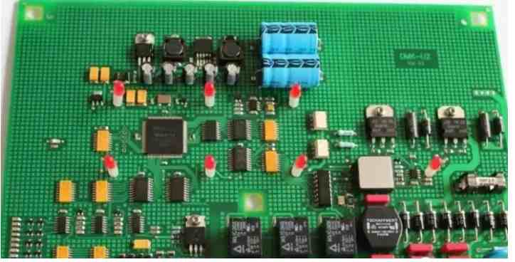
As mentioned earlier, PCBS with add-ons are called Assembly PCBS, and the manufacturing process is simply called PCB Assembly or PCBA. These tiny green chips are encapsulated in copper wires that sit in components at the center of the destroyed electronics. Their frames are made of fiberglass, copper, and other metal components, and are worn with epoxy and insulated by a solder resistance film.
On a board, copper wires called cables are electrically connected to connectors and components. These functions run signals to allow the board to operate in a specific way. These functions range from basic to complex, but the size of the PCB can still be smaller than the size of the thumbnail
Over the past few decades, the PCBA industry has evolved dramatically in terms of micro details. The two main assembly types used in the PCBA industry are as follows.
Surface Mount Technology (SMT)
Sensitive components are automatically installed on the board, such as minimum values such as resistors or diodes. Surface mount units are called SMD assemblies. It is suitable for small components and integrated circuits (ics). Some manufacturers can assemble packages in the smallest sizes. 01005, even smaller than the tip of a pen. The four main stages are as follows:
PCB organization: The assembly process begins with spreading solder paste on the board, especially in areas where solder paste is needed.
Insert the component: The next stage involves placing the component in the desired position on the board, and then completing the process using the pick and place device.
Reflow welding: After the component is inserted, heat is started using an assembler. In this process, the plate is heated inside the reflow furnace by an assembler and the process continues until a solder joint is formed. This happens by providing the desired temperature for the solder paste.
Inspection: The last step involves inspection by the assembler throughout the SMT process.") https://www.kingfordpcb.com/yuan.php
https://www.kingfordpcb.com/yuan.php
Through Hole technology (THT) Through hole technology applies to components that are connected to a conductor or cable by a hole connection. Components are assembled on one side of the board and welded on the other side. This technology is used in PCB assemblies that contain large components, such as capacitors and mounting cubes. The basic steps of this process are as follows:
Drilling: The first step in this process is to drill holes in the board. The holes to be drilled must be of sufficient size so that the components can be easily positioned.
Lead laying: This step involves laying the wire, which is done by the assembler.
Welding: This step confirms that the components used must be kept in the correct position when necessary.
The final step is inspection, a thorough inspection of the entire component to confirm that the PCBA is working properly.
Empty PCB boards are refilled or repackaged with electronic components to create a valid printed circuit board (PCA) or PCBA during assembly. With hole technology, electronic components are placed in holes surrounded by conductive pads. The SMT places the pins on the PCB to ensure that the pins match the conductive pads
Before welding, the electronic component fasteners on both sides of the circuit board must be glued to one side of the circuit board. The standard procedure for testing PCB components is as follows. Visually inspect the board with the power off or with an automatic optical inspection tool.
Shutdown is used to perform simulated signature analysis. This investigation is called a "shutdown check."
Finally, a bump test is performed to determine if the PCB is performing its job. Manufacturing process
Since PCBS do not require assembly, they are easier to manufacture. Given the complexity of PCBA, as different modules have to be connected, and with that comes oven brazing of their joints. The cost of producing a PCB for the same board is much lower than the cost of manufacturing a PCBA system. Additional PCBA projects also have a considerable cost, which adds to the total PCBA fee completed
PCB is an empty board. It has no components for transmitting electricity, instead, the PCBA is equipped with all the necessary components and can be used.
PCBS come in vacuum packaging, while PCBA boards come in isolated or antistatic packaging.
Key point: Without PCBA, PCB will not work properly
The function of the PCB can only be realized after assembly. Therefore, the terms PCB and PCBA are widely related. Some key points of this article are as follows.
Conceptual difference: PCB stands for bare circuit board, while PCBA stands for PCB board equipped with components using plug-in assembly or SMT assembly process. A PCBA should be understood as a complete circuit board, but a PCBA cannot be calculated until the board is equipped with the components required for its function. These components are usually electronic chips, cables and other electronic parts. However, because PCBS come in a variety of packages and specifications, there is more. Common PCB is made of epoxy resin glass resin, divided into 4 layers, 6 layers and 8 layers of board; Depends on the number of signal layers.
PCB is undoubtedly the basic component of all electrical systems. Our society depends on the successful implementation of the circuit board to handle affairs efficiently. If this basic technology fails, all of humanity's electrical systems will become unusable.
In general, PCB and PCBA both have latent potential. We are always moving towards better design and the ability to accommodate ultra-complex functions on small boards.


Just upload Gerber files, BOM files and design files, and the KINGFORD team will provide a complete quotation within 24h.