
Professional PCB manufacturing and assembly
Building 6, Zone 3, Yuekang Road,Bao'an District, Shenzhen, China
+86-13410863085Mon.-Sat.08:00-20:00

With the huge impact of the latest technologies such as 5G, IoT, and artificial intelligence on the world of electronics, there is a lot going on in PCB manufacturing right now. New trends in the PCB development process are quickly catching up. The global PCB market size is expected to be approximately US$70-75 billion in 2023.
Various areas related to PCBs are developing simultaneously, including: direct imaging, where circuit patterns are printed directly on the material; new materials for substrates; new methods of surface finish testing; flexible PCBs; the degree of automation of the manufacturing process; and being greener.

The root of these technology trends is the growth of market demand for PCBs.
The speed of communication is skyrocketing with the 5G technology network. IoT technologies have created specific IoT devices for nearly every industry, including industrial automation, smart homes, healthcare, and wearables. Artificial intelligence and machine learning have penetrated beyond the manufacturing or assembly floor.
Wearable devices such as glasses, chip implants or prosthetics. Self-driving technology is used to automate different levels of functions or actions, including driverless cars and drones.
PCB Development Trends Listed by Global Circuit Board Market
Different technical fields of PCB have different needs, such as changing the shape of PCB or related accessories. Recently, major advances in camera modules have been made to improve high-resolution picture and video imaging. In-vehicle cameras will become a strong demand outside of the consumer electronics and industrial sectors.
3D printed electronics (3D PE) are changing the design of electrical systems. 3D PE is an additive manufacturing process that builds 3D circuits by printing substrates layer by layer. 3D printing enables rapid prototyping in a fraction of the time. No minimum build required. With this printing technique, no plate making process is required. This will expand product functionality and improve overall efficiency due to automation.
High Density Interconnect (HDI) PCBs offer high performance and extremely thin materials compared to traditional PCBs. This provides compact routing, tiny laser vias and pads. HDI PCBs are the first choice for miniaturized electronics.
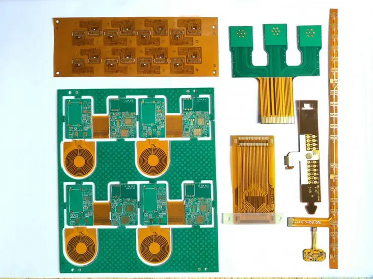
Consumer electronics is one of the fastest growing trends with the rise in cell phone and internet TV subscriptions. Wearables such as smartwatches also contributed to the expansion in the consumer segment. These applications are increasing the demand for compact, precise and versatile PCBs. Furthermore, the latest IoT applications are driving the development of flex and rigid-flex PCBs due to the durability and size advantages they offer.
The massive use of chips in the semiconductor industry has forced PCB experts to research new alternatives. Non-degradable e-waste also severely impacts the environment, leading designers to explore organic or biodegradable PCBs as alternatives.
AI-enabled solutions are now at the forefront in almost every industrial sector. AI applications are creating a need for improvements in PCB design and manufacturing processes. Focusing on accelerating development cycles to reduce defects and deliver products quickly are key goals sustained by the ever-evolving PCB industry.
Traditionally, the PCB was the passive medium used to connect the active components of a circuit design. But recently, designers have been exploring the possibility of making the PCB itself an active component of the circuit. This approach reduces component requirements while performing the required functionality.
Technology trends such as Augmented Reality (AR) and Virtual Reality (VR) are dominating the consumer electronics space and influencing PCB design to address issues such as mounting electronic packages in unconventional shapes. This will confirm correct circuit operation and reduce placement and routing requirements. In addition, AR with software simulation methods can reduce the cost of training programs because advanced simulations can replicate the actual environment of magnetic and electric fields. This will confirm that the product complies with the required regulations.
The demand for electric vehicles and autonomous vehicles is growing rapidly, and the demand for PCBs with good heat dissipation capabilities is also increasing. Advanced automotive PCB designs will address safety, convenience and environmental concerns. New energy sources such as power electronics will require PCBs with excellent thermal design. High current requirements and thermal issues should be handled during PCB design. It is mandatory to choose a reinforced PCB harness and follow an effective layout strategy.
The complex design requirements of multilayer PCB manufacturing cover all applications. PCBs in medical and aerospace applications require tight control over EMI issues. In addition, mobile phone developers need to minimize unnecessary radiation hazards. If the PCB design does not meet EMI regulations, high-volume boards may end up being redesigned, increasing costs and delaying final delivery. The growing popularity of flexible PCBs has also brought new challenges to PCB designers. The potential for electromagnetic interference between components and traces in a flexible PCB is very high, resulting in degraded performance. This issue drives the need for built-in ESD protection systems.
With the development of the trend, the speed of PCB design and development has greatly increased. But errors and debugging costs can be reduced by spending more time designing, pcb manufacturing and assembling products.
As PCB trends change with the latest technological innovations, PCB manufacturers will have to build more dynamic supply chains and PCB flexible manufacturing processes to meet the demands of these PCB trends.
Previous:No
What is a flexible circuit board (FPC)?
Oct 22,2022


Just upload Gerber files, BOM files and design files, and the KINGFORD team will provide a complete quotation within 24h.