
Professional PCB manufacturing and assembly
Building 6, Zone 3, Yuekang Road,Bao'an District, Shenzhen, China
+86-13410863085Mon.-Sat.08:00-20:00


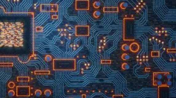
pcba processing and proofing, in order to ensure the quality of pcba, pcba transportation and storage should also strictly abide by the operating specifications. Then, what are the pcba transportation and storage requirements?
After proofing, transportation and storage requirements:
1. Use appropriate means of transport
After pcba processing and proofing, transportation tools should be ensured in good condition, such as wheels, frames, etc. Abnormal items should be reported for repair in time, and it is forbidden to use them "with injuries", so as to avoid the fall and extrusion of semi-finished products during transportation.
2. Check common tools
Transport tools, storage tools, storage and other operations should be done before cleaning, do not allow sundries, tin slag and so on. Avoid mutual friction caused by pcba processing and proofing damage.
3. Identify important information
pcba containers and tool carts for transportation and storage should be clearly marked to record product-related information to avoid misplacement or mixing.
Direct stacking of PCb as is prohibited on transportation tools, storage in turnover area and storage in working station. Especially in transportation, direct overlapping will cause damage between components.
5. Loading and unloading requirements
After pcba processing and proofing, in the process of transportation and loading and unloading, it should be safe and orderly, and it is prohibited to rough loading and unloading.
6. Prevent falls
When the pcba is stored on the transport vehicle and in the turnover area, protection should be done around it to avoid falling.
7. Prevent friction damage
During transportation, pay attention to whether the road condition is good, whether there are obstacles, potholes, etc., to avoid the damage of semi-finished products after pcba proofing caused by vehicle turbulence. The speed of the conveyance should be balanced and reasonable.
8. Transfer transportation requirements
The transfer of the board card between stations is carried out by conveyors or "hand by hand", and the overlapping placement and extrusion of semi-finished products need to be avoided. It is strictly prohibited to throw during transfer and transmission.
9. Dust proof requirements
For the storage of pcba processing and proofing semi-finished products in the turnover area, ensure that the storage tools are stable and well protected, and strictly limited in the prescribed area. The above layer should be done with dust prevention and fall prevention measures.

10. Stacking principle
Storage should pay attention to the high and low, weight and other principles, to avoid isolated single stack situation.
11. Prevent collisions
At the corner of the channel and at the end and end of the assembly line, pay attention to other pedestrians and vehicles to avoid accidental impact of other vehicles and personnel, which may cause damage to the products.
12. Prevent extrusion
Pcbas should be separated by partitions and should not extend beyond the top edge of the container to avoid squeezing.
13, workbench selection
For a large number of not suitable for storage on the workbench, should choose the appropriate container, placed around the operator, convenient access to the operator.
14. Exception handling
In case of abnormal tools during transportation, it is necessary to ensure the safety of personnel and goods, and do a good job in isolation and reporting.
General principles to be followed in the layout design of multilayer printed boards:
(1) The power layer plane should be close to the grounding plane and designed below the grounding plane.
(2) The wiring layer should be designed adjacent to the whole metal plane.
(3) digital signal and analog signal to have isolation design, first of all to avoid digital signal and analog signal in the same layer, if it can not avoid, can use analog signal and digital signal division wiring, with slot and other ways to analog signal area and digital signal area isolation. The same goes for analog power and digital power. Especially digital power, radiation is very large, must be isolated and shielded.
(4) The printed lines in the middle layer form the plane waveguide, and the microstrip lines in the surface layer form, and the transmission characteristics of the two are different.
(5) Clock circuit and high frequency circuit are the main interference and radiation sources, must be arranged separately, away from the sensitive circuit.
(6) The stray current and high-frequency radiation current contained in different layers are different, so the wiring can not be treated equally.
The electromagnetic compatibility of PCB board can be greatly improved by layer design and layer layout.
The design of layers mainly considers the power layer and ground layer, high frequency signal, special signal, sensitive signal.
The layout of the layer mainly considers various coupling, ground and power line layout, clock and high-speed signal layout, analog signal and digital information layout.


Just upload Gerber files, BOM files and design files, and the KINGFORD team will provide a complete quotation within 24h.