
Professional PCB manufacturing and assembly
Building 6, Zone 3, Yuekang Road,Bao'an District, Shenzhen, China
+86-13410863085Mon.-Sat.08:00-20:00

The definition of metal half hole (groove) is that after a drill hole is drilled and then drilled twice, the shape process will eventually retain half of the metallized hole (groove). Simply speaking, half of the metallized hole on the edge of the plate will be cut.
Plate edge semi-metallized hole process in Jialichuang qq800058721 processing is a very mature process.
How to control the quality of the product after the molding of plate edge semi-metallized hole. Such as hole wall copper spines, residual is always a difficult problem in the process of processing.
This kind of PCB with a whole row of semi-metallized holes on the edge of the board is characterized by a relatively small aperture. Most of them are used on the carrier board as a sub-board of the mother board, through which the semi-metallized holes are welded together with the pins of the mother board and components.
So if there are copper thorns in these semi-metallic holes, when welding by plug-in manufacturers, it will lead to weak welding feet, virtual welding, and serious short circuit bridging between the two pins.
In either drilling or milling, the rotation direction is clockwise. When the cutter reaches point A, the metallized layer on the hole wall is closely connected to the substrate layer to prevent metal

The extension of the chemical layer during processing and the separation of the metallized layer from the pore wall will also ensure that there will be no copper spike warping and residue after processing here. When the tool is processed to point B, due to the copper attached to the hole wall
Without any adhesion support (FIG. 1), when the tool moves forward, the metallized layer in the hole will curl along with the rotation direction of the tool under the influence of external forces, resulting in the warping and residual copper spines.
Tools and quality inspection methods for circuit board welding
Fusion welding is a process in which the interface of the workpiece is heated to a molten state and welded without pressure. In the welding process, the heat source rapidly heats and melts the joint of the two workpieces to be welded, forming a molten pool.
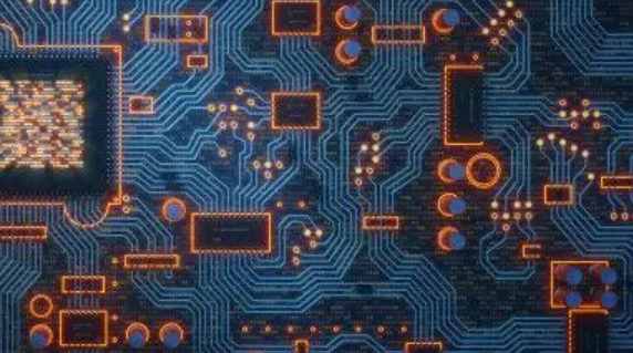
A common circuit board in life
During the welding process, if the atmosphere is in direct contact with the high-temperature molten pool, the oxygen in the atmosphere will oxidize metals and various alloying elements. Nitrogen and water vapor from the atmosphere will enter the weld pool, and during the subsequent cooling process will also form holes, slag, cracks and other defects in the weld, which will reduce the quality and performance of the weld.
What does the circuit board welder have? At present, the main use of electronic components welding technology. The welding technique uses a tin-based tin alloy material as a solder, and the solder melts at a certain temperature, and the metal solder and tin atoms attract each other, diffuse and bond together to form a wet bonded layer. It appears that the PCB's copper platinum and component leads are very smooth. They actually have a lot of tiny bumps on their surface. The molten tin solder is diffused along the surface of the solder by capillary suction to form solder and solder. The penetration of parts, assemblies and printed boards is firmly bonded and has good electrical conductivity.
Selective welding processes include flux spraying, circuit board preheating, dip welding and drag welding. Flux coating process in selective welding, flux coating process plays an important role. When the circuit board is heated and welded to be completed, the flux should have very flexible characteristics to prevent bridging and prevent oxidation of the circuit board. The manipulator sprays the flux, makes the circuit board pass through the flux nozzle, and then sprays the flux to the welding position of the PCB circuit board.
Circuit board welding quality inspection methods include appearance inspection, infrared inspection and on - line test. Among these methods, the most economical and most commonly used is the visual method, which is economical, convenient, simple and feasible. Other methods require some kind of device support. In spite of the huge investment, high inspection reliability can be guaranteed.


Just upload Gerber files, BOM files and design files, and the KINGFORD team will provide a complete quotation within 24h.