
Professional PCB manufacturing and assembly
Building 6, Zone 3, Yuekang Road,Bao'an District, Shenzhen, China
+86-13410863085Mon.-Sat.08:00-20:00

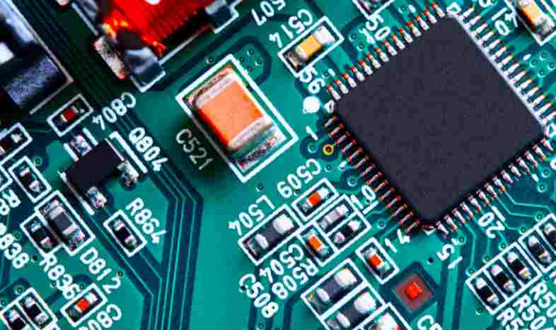
High-tech development, people need high performance, small size, many functions of electronic products, promote double-sided circuit board manufacturing also to light, thin, short, small development, limited space, to achieve more functions, circuit board drawings wiring density increases, aperture is smaller. Between 1995 and 2005, the minimum bore capacity of the mechanical drilling lot decreased from 0.4mm to 0.2mm or even smaller. The size of the metallization hole is also getting smaller. Layer to layer interconnection depends on metallized holes, quality is directly related to the reliability of printed board. With the reduction of the aperture, the original debris that has no effect on the larger aperture, such as brush debris and volcanic ash, once remaining in the hole, will make the chemical precipitation of copper, electroplating of copper will lose effect, the hole without copper, become the fatal killer of hole metallization.
When the holes in the circuit board appear to plug holes, due to the small aperture, it is difficult to remove the impurities in the holes by high pressure washing and chemical cleaning before copper deposition, which prevents the exchange of traditional Chinese medicine water in the holes in the process of chemical copper deposition, so that the chemical copper deposition loses its effect. When drilling, appropriate drill nozzle and pad should be selected according to the thickness of the stack, so as to keep the substrate clean and not reuse the pad. Effective suction effect (using an independent suction control system) is a factor that must be considered to solve the plug hole.

By what is the perforation design of high speed PCB circuit board implemented in the production process?
For the design of holes in high-speed PCB, most of them are based on the analysis of the parasitic characteristics of holes. We can see that, usually in the process of high-speed PCB design, the seemingly simple holes usually bring great negative effects to the circuit design.
Therefore, in order to reduce the adverse effects brought by the parasitic effect of holes, we can try to do the following points in the design:
1, whether from the point of view of cost and signal quality, select a reasonable size of the hole. For example, for the design of 6-10 layers of memory module PCB, it is better to choose 10/20Mil (drill/pad) pass hole, for some small high-density circuit boards, you can also try to use 8/18Mil pass hole. Under current technical conditions, it is more difficult to use the smaller size of the hole. For the power supply or ground wire hole can be considered to use a larger size, in order to reduce the impedance.
2. It can be concluded from the above discussion that the use of thinner PCB board is conducive to reducing the two parasitic parameters through the hole.
3. The signal line does not change on the PCB layer, that is to say, try not to use unnecessary holes.
4. The pins of the power supply and the ground should be drilled nearby. The shorter the lead between the hole and the pin, the better, because they will increase in the inductance. At the same time power and ground leads should be as thick as possible, in order to reduce impedance.
5. Place some grounding holes near the signal switching holes, in order to provide the latest signal circuit. You can even put a lot of extra ground holes on the PCB board. Of course, it also needs to be flexible in design.
The hole model discussed above is that everyone has a pad case, and sometimes, we can reduce some of the keyboard or even eliminate the layer. Especially in the case of very large hole density, it may lead to the formation of a cut off loop in the copper layer. To solve this problem, in addition to moving the position of the hole, it is also possible to consider the through hole in the pad, in order to reduce the size of the copper layer.
Unique production line insight allows you to understand the different PCB
In Asia, we have long been used to the configuration of mass production of a dragon assembly line, each operator only assembles a few PCB parts, complete their own work, to say the best is to let each operator as soon as possible to master their own work content, to say the worst is to use the operator as a robot. If you look at the electronic assembly and manufacturing factories all over the world, you will find that the production lines of many electronic assembly plants are not necessarily the same as those we are familiar with. Some PCB factories do not necessarily adopt assembly lines, especially in Europe, and some factories do not necessarily have to fix parts in front of the operators. Have you ever thought that the current assembly line is the best way to work?
Today we will introduce an assembly Line called Sushi Box Production Flow Line. This may be the process we named ourselves, because we can't see other production lines with such a name, because the static material boxes used for turnover are like sushi sets of Japanese food, so named.
This sushi box is designed to hold all the parts of a whole product inside, which means that a person must place all the parts of a whole product inside the sushi box in the material area, and then the water spider will place the sushi box on the flow line of the product assembly line, usually with a slanted table with a pulley. The sushi box can slide along with the flow of product assembly. Each operator takes the components in the sushi box in order, and then installs the product. When the product is assembled, the parts in the sushi box are just used up.
The advantages of using linear assembly of sushi boxes include reducing and reducing the chance of missing PCB parts. Such problems usually occur in some operators quality uneven countries or regions, often in central and South America, often found after the completion of product assembly problems. It can increase the efficiency of assembly personnel and reduce the manpower of production line. Because all the materials are placed in the sushi box, the production line operators only need to take parts from the sushi box in order to assemble, do not have to remember which parts installation sequence, relative to each station operators can install the number of parts can be increased, IE or process engineers can be more efficient arrangement of product assembly sequence.
The relative waiting time between stations can also be reduced, thus increasing the efficiency of output. Reduce the production line material accumulation dirty problem. This method is very heavy responsibility of the material clerk, who must first prepare all the materials in the material area and put them into the sushi box, so the assembly line looks very clean, no excess material accumulation problem.


Just upload Gerber files, BOM files and design files, and the KINGFORD team will provide a complete quotation within 24h.