
Professional PCB manufacturing and assembly
Building 6, Zone 3, Yuekang Road,Bao'an District, Shenzhen, China
+86-13410863085Mon.-Sat.08:00-20:00


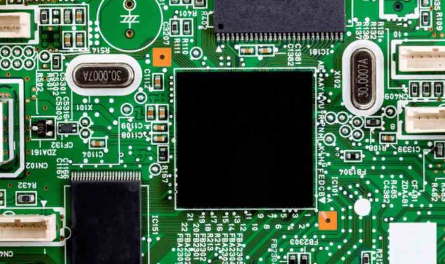
Multilayer circuit board is a structural component composed of a dielectric layer and a circuit, and the circuit is arranged on the surface and inside the dielectric material. In the Design work, there must be a common size planning criteria, otherwise most of the electronic components on the market cannot reach the common, such wiring Design Rule is the design rule of the PCBA board.
1 Grid
Because the positions of all components on the circuit board are relative coordinates, the original idea of circuit board circuit collocation is to allocate blocks on the board plane with assumed grid lines. Since the circuit boards were first dominated by European and American countries, the early specifications were 1/10-inch in size, while the metric system was 2.5mm in size, which was equivalent to l00mil in the British system. On this basis, the different spacing is divided to make the position configuration of the hole and the copper pad, which is the traditional design principle of the through-hole element. However, after the popularity of SMT- Surface Mount Technology, it is impractical to configure holes on the grid points. Although there are lattice points in the design, the actual design is not limited by lattice points. The holes are more and more for the purpose of conduction, and the blind and buried holes have nothing to do with lattice points.
The most influential part of this change is the electrical test, because the traditional electronic component contact is based on the design of grid points, so whether drilling or welding points are based on grid points. Therefore, the circuit board following the lattice design can use the so-called Universal Tool for electrical test, but after the lattice principle is broken, the test must move to a more dense contact form, so a small number of products began to use the so-called Flying Probe test. In mass production, Dedicate tools were used for testing.
2 Line width spacing
The design of thin wire becomes the inevitable trend of the development of high density circuit board, but the design of thin wire must consider the change of resistance, characteristic impedance and other factors. The size of the line spacing is subject to the insulation of the dielectric material. For organic materials, about 4 mil can be selected as the target value. Due to the development of product demand and process technology, products with spacing of about 2mil or less are entering the practical application. In the face of further compression of the line spacing of semiconductor packaging board, how to maintain the due insulation has become a subject that must be worked hard. Fortunately, the operating voltage of most high-density packaging boards is also relatively reduced, which is fortunate.
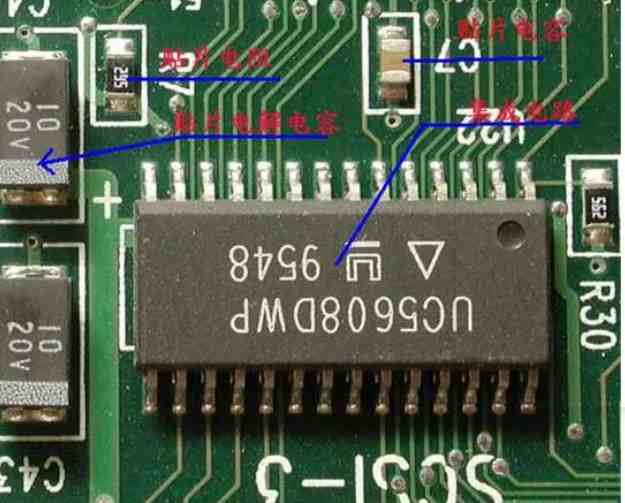
3. Diameter of microhole and diameter of copper pad
When the PCB board is mainly designed to adhere to the surface, the plating hole in addition to the interlayer connection is still partially used for plug-in function.
The structure of the table has through holes and blind holes. The holes buried in the plate are called Interstitial Via holes by some people. It is a circuit board connected between layers of microholes after the inner plate with plated through holes is pressed together. The production of these microholes is designed with a small diameter in order to play the space saving work. Generally, it is economical to drill holes larger than 8mil by mechanical drilling, although it is now claimed that it can be done. 4 mil of products, but the cost is too high and not practical.
Due to the limitations of mechanical aperture and production rate, boards using the additive layer method will not only use microporous technology on the surface, but also be designed to be smaller in terms of the internal through holes to increase density. The aperture reduction greatly increases the degree of freedom of line configuration, and the high density and layer circuit board is popularized.
4 interlayer structure
The design of multilayer circuit board depends on the allowable wiring density. In the past, the circuit board to four boards, mainly from the signal line needs electromagnetic shielding, not from the winding density. Due to the increasing complexity of electronic components, the original winding density and level design can no longer meet the needs, so the level is gradually improved. However, since increasing the number of layers would increase the production cost, we tried to reduce the number of layers in the initial design. Therefore, with more microholes and fine lines, the element can still be achieved in a limited number of layers. Piece connection. Even so, with the advancement of semiconductor components, the total number of layers on the circuit board is still gradually climbing.
In the aspect of circuit structure, due to the continuous increase of the overall power of electronic products, transmission rate is also increasing, so in the limited space and to maintain the conductor cross-sectional area, many designs will require a higher line thickness but also to make a thinner line. There are also strict restrictions on the control of the thickness of the interlayer dielectric layer and the allowable error, so the configuration of the inner substrate and film becomes very important. General PCB circuit board pressing structure will use symmetrical design, this is in order to reduce stress uneven consideration.
For products that require stringent electrical characteristics, the correct integration of characteristic impedance and the allowable tolerance of the thickness between the power supply and the ground layer becomes more stringent. Therefore, many production procedures are to make the key thickness layers to the substrate first, and the less important layers are handed over to the film to complete, because the substrate has been hardened in advance can be used to select the substrate to the specification of the production, so it can improve the yield and electrical performance.
In the design of high density laminated circuit board, it is necessary to determine the number of line layers according to the winding density, and to determine the wiring mode, layer thickness, line width thickness by electrical characteristics. In order to prevent bending and warping of the plate, symmetrical pressing design should be used as far as possible. Generally, the power supply and grounding layer of high-density laminates are mostly located on the inner hard board, and the signal layer is made of laminates to integrate impedance characteristics, but this rule may not be followed for higher level products.


Just upload Gerber files, BOM files and design files, and the KINGFORD team will provide a complete quotation within 24h.