
Professional PCB manufacturing and assembly
Building 6, Zone 3, Yuekang Road,Bao'an District, Shenzhen, China
+86-13410863085Mon.-Sat.08:00-20:00

Laser marking is a very advanced marking technology, through focusing laser engraving technology, will need to mark the character, pattern engraving on the surface of the object. Compared with the traditional printing technology, laser marking has the characteristics of good quality, high consistency, strong wear resistance, high efficiency, cost saving and safety and reliability, and is widely used in the printed circuit board(PCB) industry.
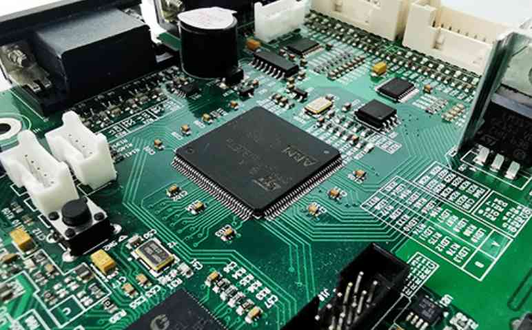
With the rapid development of the IT industry, smart phones, wearable electronics and other products continue to be thin and miniaturized. Consumers have higher and higher requirements for electronic products, and the production of PCB board must be kept improving. In order to realize the quality control of PCB board production process, marking characters, one-dimensional codes, two-dimensional codes and other information on PCB board for traceability has become the development trend of the industry.
Because of poor wear resistance, low precision, poor aesthetics, environmental pollution and other problems, traditional printing technology is increasingly unable to meet the needs of new market technology. Therefore, laser marking has become a trend in PCB industry.
The defects of traditional printing technology
In the past, silk screen printing in traditional printing was usually used for marking like pattern drawing, company LOGO printing, contact information and two-dimensional code on the surface of PCB board. Under the original market demand, the traditional printing technology can also meet the requirements of the market, but with the continuous improvement of the quality of electronic products, consumers have higher and higher requirements, resulting in the market for PCB circuit board marking quality is becoming higher and higher, the traditional printing technology can not meet the new market requirements, its shortcomings are becoming more and more obvious, such as:
1. Poor wear resistance, the wear resistance here is not the wear resistance of metal materials, refers to the circuit board surface ink in use will often be worn off causing blur, fading and so on.
2. Aesthetic requirements. The appearance of metal surface printing feels relatively low-end, which is not suitable for some products with high appearance requirements, such as commemorative badges, metal business cards, exquisite company publicity nameplates, handicraft description nameplates, etc., which cannot meet their appearance requirements.
3. In the ordinary printing process, chemical raw materials such as organic solvents and heavy metal elements are required to be used, which have certain toxicity and will cause personal injury to screen printing staff. In addition, during the drying process of screen printing ink, volatile chemical raw materials gradually evaporate into the air, causing pollution to the air and environment.
Laser marking has unique advantages
The emergence of laser marking technology has successfully solved a series of problems existing in traditional printing technology. It is characterized by high marking precision, fast speed and stable performance. And only need to be controlled by the computer, simple operation, can print a variety of complex patterns, text, two-dimensional code and other content, fully in line with the existing circuit board industry high quality marking requirements.
Compared with traditional printing technology, laser marking technology has many advantages:
1. Good quality, strong wear resistance. PCB board surface marking clear and beautiful, can mark a variety of LOGO, pattern, two-dimensional code, text and the pattern is directly carved on the material, wear resistance is more prominent;
2. High machining precision. After the laser beam is focused, the minimum spot diameter can reach 10um(UV laser), which has a small benefit in the processing of complex graphics and precision machining.
3. High efficiency, simple operation and cost reduction. Users only need to set the parameters on the computer to mark directly, in just a few seconds to more than ten seconds to complete the material surface marking.
4. Mark without damage. Laser marking using non-contact processing, laser head does not need to contact the surface of the material, so do not need to consider the damage to the material;
5. Wide range of use, safety and environmental protection. All kinds of thin metal/non-metal materials can be marked;
6. Stable performance and long service life of equipment. With the development of technology, the service life of laser is greatly increased, and the service life of equipment is greatly extended.
Application of UV laser marking and CO2 laser marking technology in PCB industry
In the laser marking application of PCB board, UV laser marking and CO2 laser marking are the most used. UV laser marking and CO2 laser marking have become the preferred technology for PCB surface marking because of their low thermal effect, good processing effect, high precision and fast speed.
The use of laser two-dimensional code marking technology in PCB industry can realize the traceability of PCB production, process and quality, and realize the requirements of automatic and intelligent management to meet the needs of lean production, quality control and process improvement. Marking two-dimensional code on PCB surface is a common demand of middle and high-end customers at present, and has been widely used.


Just upload Gerber files, BOM files and design files, and the KINGFORD team will provide a complete quotation within 24h.