
Professional PCB manufacturing and assembly
Building 6, Zone 3, Yuekang Road,Bao'an District, Shenzhen, China
+86-13410863085Mon.-Sat.08:00-20:00

Because we are a PCBA factory, customers often come to consult about relevant matters. They come from a variety of positions, from purchasing, engineering, administration, and possibly business. There are those who know and those who don't. Most likely everyone will ask about the price. So what are the factors that affect the price of a PCB board? Today we'll break it down with you.
1. Differences in PCB materials
We take: the most common double panel as an example, board material generally FR4 (Sheng Yi, Kingboard, Guoji), board thickness from 0.2mm to 3.0mm, copper thickness from 0.5oz to 3oz range, all these in a board, may cause a very large price difference; In addition, in the welding ink, the use of the most common thermosetting oil and the use of sensitive green oil on the price also has a certain impact.
2. Differences in surface treatment technology
Common are: lead spray tin, lead-free spray tin (environmental protection), gold plating, gold plating, OSP (antioxidant), in addition to some combination of processes and so on, each of the above process differences have a great impact on the price, such as gold plating process may be more than a little bit more expensive than lead spray tin.
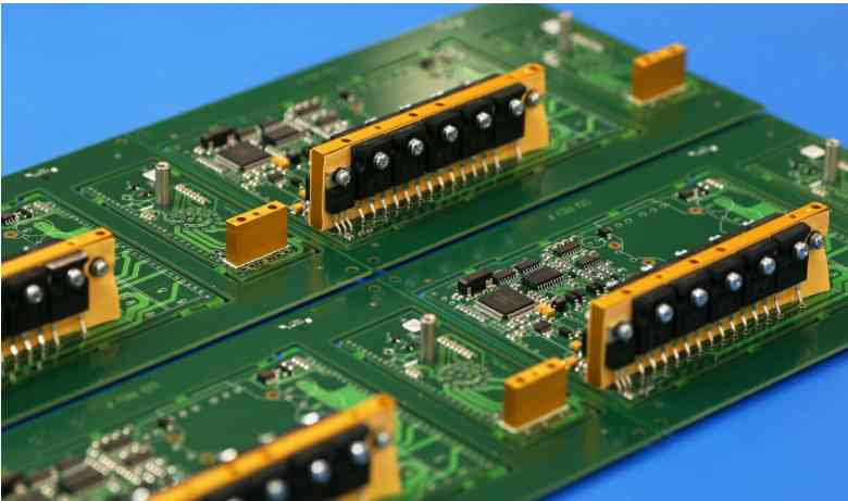
PCB inspection
3. Differences in PCB difficulty
We take a plate aperture greater than 0.2mm and another plate aperture less than 0.2mm for comparison, if it is necessary to play 1000 holes, then these two specifications of holes will form different drilling costs; In the other case, other parts of the two types of circuit board are the same, but the line width and line distance are different. One is all greater than 4mil, and the other is all less than 4mil. Such a small difference will have a great impact on the price.
Secondly, some circuit board process is not a conventional process, nor is it an ordinary processing process, the design is also to add money, such as half hole, buried blind hole, disc hole, keyplate printing carbon oil and so on.
4. Difference in copper foil thickness
Common copper platinum thickness: 1/2OZ, 1OZ, 2OZ, 3OZ, 4OZ, etc., the more expensive the above copper foil thickness, this should be easy to understand, because the thicker the copper, the more materials consumed the higher the price!
5. Customers' differences in quality acceptance standards
Commonly used are: IPC2, IPC3, enterprise standard, military standard and so on, different standards require different content, the corresponding control of details and the good and bad use of materials also have requirements, the price will be different
6. Cost of mold and test stand
(1) Mold cost. For PCB mass production, generally, factories need to open molds and flush plates, and at the same time, the cost of a set of molds is generally quoted by board factories above 1000 RMB. If some factories fail to quote, this price may have been divided into the whole batch price. There will be no additional milling charges.
(2) Test fee: PCB board is required to use flying needle test, board factory flying needle test will generally charge 100-400 yuan test fee; When mass production is to open the test rack to test, the price of the test rack is generally between 1000-1500 yuan.
7. Differences in payment methods
Considering the risks and cash flow pressure brought by the payment period to the company, different companies will have certain differences in the price of different payment methods. Just like bank payment, the shorter the time of payment to the account, such as cash payment, the lower the price may be. Of course, this is not certain.
8. The intensity of order quantity and delivery time
The fewer the quantity, the more expensive the price. Many customers do not understand, I do a piece ah, how do you charge so much. What's the reason?
Because even if you make 1PCS, the plate factory has to go to all hands. Engineering data, film, testing and inspection, packaging and delivery of a process can not run.
(2) The tension of the delivery time: PCB board is a fine work that needs time to run the process, each work can not be omitted, after all, people's energy is limited, eating, drinking and excreting all need time, if the construction period is very rushed, then you need to add people rotation, corresponding will increase the labor cost, so the price will increase.

2. Cause analysis of tin bead produced by PCBA wave soldering
Analysis on the causes of tin beads produced by wave soldering of PCBA.
Solder spatter may occur on solder surfaces and component surfaces of PCBA during wave soldering. It is generally believed that if there is water vapor remaining on the PCB before it enters the crest, once it makes contact with the solder on the crest, it will evaporate into steam for a very short time at high temperatures. Rise, resulting in a burst exhaust process. It is this intense exhaust that causes small accidents inside the weld in the molten state, causing solder particles to escape from the weld and thus splash onto the PCB.
Before PCBA wave soldering, PCBA manufacturers summarize the following conclusions:
1. Manufacturing environment and PCB storage time.
The manufacturing environment has great influence on the welding quality of electronic components. High humidity in the manufacturing environment, long time of PCB packaging and opening after SMT patch processing and PCBA wave soldering production, or PCB patch and insert after a period of time for PCBA wave soldering, these factors may produce tin beads in the PCBA wave welding process.
2. PCB resistance welding materials and production quality.
The solder film used in PCB manufacturingis also one of the reasons for the tin ball in PCBA wave soldering. Because of the affinity between the welding film and the flux, the processing of the welding film often leads to the attachment of the welding bead, which leads to the generation of the welding ball.
3, the correct choice of flux.
There are many reasons to solder balls, but flux is the main one.
General low-solid, no-clean fluxes tend to form solder balls when underside SMDS require dual PCBA wave soldering because these additives are not designed to be used for long periods of time. If the flux sprayed on the PCB has been used up after the first wave crest, there is no flux available after two peaks, so it cannot function as flux and help reduce the tin balls. One of the main ways to reduce the number of balls is to choose the right flux. Choose a flux that can withstand heat for longer periods of time.


Just upload Gerber files, BOM files and design files, and the KINGFORD team will provide a complete quotation within 24h.