
Professional PCB manufacturing and assembly
Building 6, Zone 3, Yuekang Road,Bao'an District, Shenzhen, China
+86-13410863085Mon.-Sat.08:00-20:00

First, SMT is one of the basic components of electronic components, known as surface assembly technology (or surface mounting technology), is divided into no pin or short lead, is through reflow welding or dip welding to be assembled circuit assembly technology, is also the most popular technology and process in the electronic assembly industry.
Features: Our substrate, can be used for power supply, signal transmission, heat dissipation, provide structural role.
Characteristics: Can withstand curing and welding temperature and time.
The flatness meets the requirements of manufacturing process.
Suitable for repair work.
Suitable for substrate manufacturing process.
Low dielectric number and high resistance.
The commonly used materials of our product substrate are epoxy resin and phenolic resin, which are healthy and environmentally friendly. They have good fire-proof characteristics, temperature characteristics, mechanical and dielectric properties and low cost.
That said, the rigid substrate is solid.
Our products also have flexible substrate, space saving, folding or turning, moving use, made of very thin insulation sheet, has good high frequency performance.
The disadvantage is that the assembly process is difficult and not suitable for micro-spacing applications.
In my opinion, the characteristics of the substrate are small lead and spacing, large thickness and area, good thermal conduction, hard mechanical properties, and good stability. I think the mount technology on the substrate is electrical performance, has reliability, standard parts.
We not only have automatic integration of the operation, and through the manual layer by layer of audit, machine audit manual dual guarantee, the qualified rate of products as high as 99 percent
Two, PCB is the most important electronic components, no one. Usually on the insulation material, according to the predetermined design, made of printed circuit, printed components or a combination of the conductive graphics known as printed circuit. The conductive graphics that provide electrical connections between components on the insulating substrate are called printed circuit boards (or printed circuit boards), which are important supporting bodies of electronic components and carriers that can carry components.
I think we usually open a computer keyboard and see a soft film (flexible insulating material) printed with a silver (silver paste) conductive pattern and a health pattern. Because of the general screen leakage method to get this pattern, so we call this printed circuit board flexible silver printed circuit board. And we go to the computer city to see a variety of computer host boards, graphics cards, network cards, modems, sound cards and household appliances on the printed circuit board is different.
The substrate used is made of paper base (usually used for single side) or glass cloth base (usually used for double side and multilayer), prepreg phenolic or epoxy resin, one or both surface layers glued to a copper sheet and then laminate and cure. This kind of circuit board covered with copper sheet plate, we call it rigid plate. To make printed circuit board, we call it rigid printed circuit board.
Single-side printed circuit board we call single-side printed circuit board, double-side printed circuit board, and then through the metallization of the hole for double-side interconnection, we call it a double panel. If a double-sided for the inner layer, two single-sided for the outer layer or two double-sided for the inner layer, two single-sided for the outer layer of the printed circuit board, through the positioning system and insulating binder material alternating together and conductive graphics in accordance with the design requirements of the interconnected printed circuit board will become a four-layer, six-layer printed circuit board, also known as the multi-layer printed circuit board.

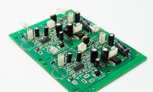
PCBA is one of the basic components of electronic components, PCB it through surface assembly technology (SMT), and the whole process of DIP plug-in insertion, known as PCBA process. It's actually a printed PCB. There's a finished board and there's a bare board.
PCBA can be understood as finished circuit board, that is, PCBA can only be counted after all the processes of the circuit board have been completed. Due to the continuous miniaturization and refinement of electronic products, most of the current circuit boards are attached to etching inhibitors (pressed film or coating), after exposure development, and then to etching circuit boards.
In the past, the understanding of cleaning is not enough, because the assembly density of PCBA is not high, and it is also believed that the flux residue is non-conductive and benign, and will not affect the electrical performance.
Electronic assemblies now tend to be miniaturized, even smaller devices, or smaller spacing. Pin and pad are closer and closer, now the gap is smaller and smaller, pollutants may also be stuck in the gap, which means that relatively small particles, if remaining between the two gaps, may also cause short circuit adverse phenomenon.
In recent years, the electronic assembly industry for cleaning awareness and voice is more and more high, not only the requirements of the product, but also the requirements of the environment and the protection of human health also have higher requirements. Therefore, there are many suppliers of cleaning equipment and solutions, and cleaning has become one of the main contents of technical exchanges and discussions in the electronic assembly industry.
DIP is one of the basic components of electronic components, known as dual-in-line package technology, refers to the dual-in-line package of integrated circuit chips, which are also used in most small and medium-sized integrated circuits, and the number of pins generally does not exceed 100.
The DIP package technology CPU chip has two rows of pins that need to be plugged into the chip socket that has the DIP structure.
Of course, it can also be inserted directly into the circuit board with the same number of welding holes and geometric arrangement for welding.
Special care should be taken when inserting and removing the DIP package technology from the chip socket to avoid damaging the pins.
Features: multi-layer ceramic double-in-line DIP, single-layer ceramic double-in-line DIP, lead frame DIP (including glass ceramic sealing type, plastic encapsulation structure type, ceramic low-melt glass packaging type) and so on.
DIP plug-in is a part of the electronic manufacturing process. There are manual plug-ins and AI plug-ins. Insert the specified material into the specified position. Handmade plugins also have to be wave-welded, where electronic components are welded to the board. The components that have been inserted should be checked to see whether they are improperly inserted or missed.
DIP plug-in post welding is a very important process in the processing of pcba patch. Its processing quality directly affects the function of pcba board, and its importance is very important. Then after welding, because some components, according to the limitations of process and materials, can not be welded by wave welding machine, can only be completed by hand.
This also reflects the importance of DIP plug-in in electronic components, only pay attention to details, can be 100 dense.
In these four electronic components, each has its own advantages, but they complement each other, in order to form a series of product production process, only on the quality of production products, in order to let a wide range of users, customers realize our intentions.
Which parts constitute the price of PCB board?
Feb 20,2023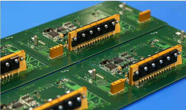


Just upload Gerber files, BOM files and design files, and the KINGFORD team will provide a complete quotation within 24h.