
Professional PCB manufacturing and assembly
Building 6, Zone 3, Yuekang Road,Bao'an District, Shenzhen, China
+86-13410863085Mon.-Sat.08:00-20:00

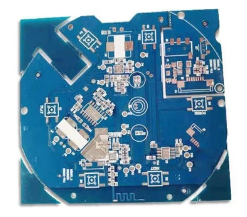
PCB board has single-sided, double-sided and multi-layer, which the number of layers of the multi-layer board is not limited, there are more than 100 layers of PCB, and the common multi-layer PCB is four layers and six layers of the board. So why do people ask, "Why are PCB multilayers even?" What about this question? Relatively speaking, PCB with even layers does have more advantages than PCB with odd layers.
1, the cost is lower because there is less a layer of medium and coating foil, the cost of raw materials of odd PCB board is slightly lower than that of even PCB board. But the processing cost of odd layer PCB is obviously higher than that of even layer PCB. The inner layer has the same processing cost, but the foil/core structure significantly increases the processing cost of the outer layer. Odd layer PCB needs to add non - standard laminated core layer bonding technology on the basis of nuclear structure technology. Compared with the nuclear structure, the production efficiency of the plant adding foil outside the nuclear structure will decrease. Prior to laminating, the outer core requires additional processing, which increases the risk of scratches and etching errors on the outer layer.
2, balanced structure to avoid bending the best reason not to design PCB with odd layers is: odd layer circuit boards are easy to bend. When the PCB is cooled after the multilayer line bonding process, the different lamination tension between the core structure and the foil-coated structure can cause the PCB board to bend. As the board thickness increases, the risk of bending increases for composite PCB boards with two different structures. The key to eliminating circuit board bending is to use balanced layering. Although PCBS with a certain degree of bending meet the specification requirements, subsequent processing efficiency will be reduced, resulting in increased costs. Because assembly requires special equipment and technology, the accuracy of component placement is reduced, so the quality will be damaged.
To put it in a more understandable way: In PCB process, four-layer board is easier to control than three-layer board, mainly in the aspect of symmetry, the warpage degree of four-layer board can be controlled below 0.7% (IPC600 standard), but when the size of three-layer board is large, the warpage degree will exceed this standard, which will affect the reliability of SMT and the whole product, so general designers, Do not design odd layer, even if the odd layer to achieve the function, will be designed as false even layer, that is, 5 layers designed into 6 layers, 7 layers designed into 8 layers of board. For the above reasons, PCB multilayer boards are mostly designed with even layers, and odd layers are less.
How to balance layering and reduce costs with odd PCB layers? What if there are an odd number of PCBS in the design? The following methods can be used to balance layering, reduce PCB production costs and avoid PCB bending.
(1) A signal layer and utilization. This method can be used if the PCB is designed with even power layers and odd signal layers. The additional layer does not increase the cost, but can shorten the lead time and improve PCB quality.
(2) Add an additional power layer. This method can be used if the PCB is designed with odd power layers and even signal layers. An easy way to do this is to add a layer in the middle of the stack without changing the other Settings. Route an odd number of PCB layers first, then duplicate layers in the middle and label the remaining layers. This is the same electrical property as the coating of thickened layers.
(3) Add a blank signal layer near the center of the PCB stack. This method minimizes stack unbalance and improves printed circuit board quality. The odd-numbered layers are routed, and a blank signal layer is added to mark the remaining layers. In microwave circuits and mixed media (media with different permittivity) circuit types are used.
The Great life of Paul Essler, the Father of PCB
Feb 21,2023


Just upload Gerber files, BOM files and design files, and the KINGFORD team will provide a complete quotation within 24h.