
Professional PCB manufacturing and assembly
Building 6, Zone 3, Yuekang Road,Bao'an District, Shenzhen, China
+86-13410863085Mon.-Sat.08:00-20:00

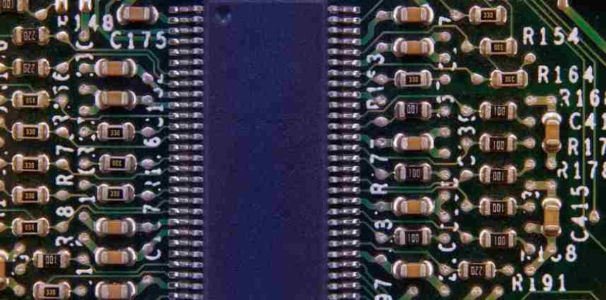
PCB (Printed Circuit Board), the Chinese name is called printed circuit board, also known as printed circuit board, is the support body of electronic components, is also the carrier of electrical connection of electronic components. In the electronics industry, almost every kind of electronic equipment, from small electronic watches and calculators to large computers, communication electronic equipment and military weapon systems, as long as there are electronic components such as integrated circuits, in order to make the electrical interconnection between each component, PCB is used.
PCB industrial chain
The industrial chain of PCB from top to bottom is as follows: upstream raw materials -- midstream manufacturing -- downstream PCB application A remarkable feature of PCB is the wide coverage of downstream applications, covering computer, communications, consumer electronics, industrial control medical, military, semiconductor and automotive industries, almost involving all electronic information products. Among them, computer, communication and consumer electronics are the three main application fields, accounting for about 70% of the output value of PCB industry.
Classification of copper-clad plates
Copper coated plate (CCL) is the upstream core material of PCB manufacturing. It is a plate-like material made by dipping electronic glass fiber cloth or other reinforcing material with resin, covering one or both sides with copper foil and pressing hot. It accounts for about 20% ~ 40% of the production cost of PCB, and has a strong interdependence with PCB.
1) in accordance with the mechanical rigidity can be divided into rigid copper clad sheet (RigidCopperCladLaminate) and flexible copper clad (FlexibleCopperCladLaminate).
2) According to different insulating materials and structures, it can be divided into organic resin copper-clad plate, metal base copper-clad plate and ceramic base copper-clad plate.
3) According to the thickness of copper clad plate, it can be divided into thick plate (plate thickness range is 0.8 ~ 3.2mm (including Cu)) and thin plate (plate thickness range is less than 0.78mm (excluding Cu)).
4) According to the reinforcing material of the copper clad plate, it can be divided into glass cloth copper clad plate, paper copper clad plate and composite copper clad plate (CME-1, CME-2).
5) Divided into flame retardant plate and non-flame retardant plate according to flame retardant grade: In accordance with the provisions of UL standards (UL94, UL746E, etc.), the flame retardant grade of CCL is divided into four types of rigid CCL flame retardant grade: UL-94V0; UL-94V1; UL-94V2 and UL-94HB.

PCB design
PCB design belongs to a development link of product hardware design and is an important research and development work connecting the schematic design of hardware circuit board and circuit board processing and manufacturing. Its project flow is as follows:
1) At the beginning of the project, it is necessary to check whether all the materials required by the project are complete, including schematic diagram, structural diagram, packaging library, signal flow diagram of complex products, power tree diagram, key signal description, power current size, design requirements, etc.
2) Design information input: including the import of netlists and structure drawings. After the structure drawing is imported, special attention should be paid to the size of screw holes and some positioning holes, the forbidden area of devices and cables, the height limit area, and the location of connectors.
3) Layout: On the basis of comprehensive consideration of signal quality, EMC, thermal design, DFM, DFT, structure, safety and other requirements, the device is placed on the board reasonably. The basic idea of layout is to combine signal flow direction and power flow direction in addition to the structural limitations.
4) Wiring constraints: Wiring constraints are mainly divided into line width, spacing size, equal length, etc. Some rules need to be guided by pre-simulation, such as line length, impedance size, topology, and cascading structure.
5) Wiring: Wiring is the most workload of PCB design, there are a lot of places to pay attention to. Such as line impedance, continuity of reference surface, EMC, SI/PI, DFM, etc.
6) Review + post-simulation verification: After wiring is completed, review and inspection by senior personnel of the department and simulation of key signals and power supply are required.
7) Processing: After the PCB design is OK, the light drawing file can be output for production.
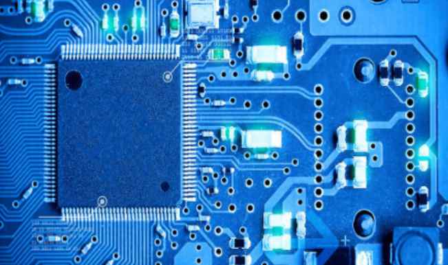
PCB processing
PCB processing and manufacturing processes are more, whether it is line processing, solder printing ink processing, silk screen processing, are similar to the way of "printing", which is also the reason why PCB is called "printed circuit board" or "printed circuit board".
The importance of cleaning printed circuit boards
For the manufacture of PCB boards, most people focus on the actual design, as this has the greatest impact on the performance of the board. However, there are several other very important factors to consider when making printed circuit boards.
One of these key qualities is to make sure the PCB is as clean as possible. This should always be done when acquiring these products from any good printed circuit board company. However, it's important for you to know why it's so important to have clean printed boards and what happens when you allow them to get dirty.
Problems caused by excessive accumulation of dust
One function that is used every time in the PCB board manufacturing process is flux. This is because it must be possible to properly wet the metal solder and form a metallurgical bond. But because of this process, some residual flux is sometimes left behind. Once this happens, it will start to attract dust and coat the PCB with a thin layer of dust much faster than it would otherwise.
This often results in the MCU being negatively impacted. These microcontroller units are generally considered capable of operating at voltages between 0 and 5v. However, once some dust or moisture is introduced into the PCB, it immediately affects the level of voltage that can be transmitted and greatly increases the chance of a short circuit forming.
Another way dust can negatively affect these PCBS is by suppressing airflow levels, which causes the heat generated by the various components to disperse at a very slow rate. Therefore, good PCB manufacturing is easy to be destroyed by dust accumulation.
What does excessive humidity cause
With regular use and cleaning of PCBS, humidity levels may not rise to dangerous levels. This changes, however, once PCBS are left uncleaned for a long period of time, when their humidity reaches levels that can cause oxidation.
10 practical ways to cool PCBS
Feb 11,2023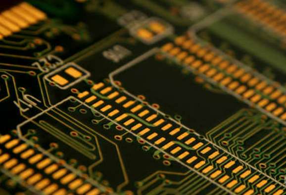


Just upload Gerber files, BOM files and design files, and the KINGFORD team will provide a complete quotation within 24h.