
Professional PCB manufacturing and assembly
Building 6, Zone 3, Yuekang Road,Bao'an District, Shenzhen, China
+86-13410863085Mon.-Sat.08:00-20:00

For electronic equipment, a certain amount of heat will be generated during work, so that the internal temperature of the equipment will rise rapidly. If the heat is not dissipated in time, the equipment will continue to heat up, and the devices will fail due to overheating, and the reliable performance of electronic equipment will decline.
Therefore, it is very important to have a good heat dissipation treatment on the circuit board. The heat dissipation of PCB circuit board is a very important link, then PCB circuit board heat dissipation skills are what, let's discuss the next.
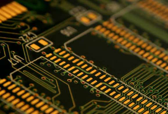
1, through the PCB board itself heat dissipation is currently widely used PCB board is covered with copper/epoxy glass cloth substrate or phenolic resin glass cloth substrate, there is a small amount of paper covered with copper plate.
Although these substrates have excellent electrical properties and processing properties, but poor heat dissipation, as a heat dissipation way of high heating components, almost can not be expected from the PCB resin conduction heat, but from the surface of the components to the surrounding air heat dissipation.
However, as electronic products have entered the era of component miniaturization, high-density installation and high thermal assembly, it is not enough to only rely on the surface of components with very small surface area to dissipate heat.

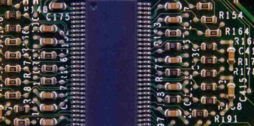
At the same time, due to the large number of surface mounted components such as QFP, BGA, the heat generated by components to PCB board, therefore, the best way to solve the heat dissipation is to improve the heat dissipation capacity of PCB in direct contact with the heating element, through the PCB board conduction out or out.
Add heat dissipation copper foil and use large area power source copper foil
Heat through hole
IC back exposed copper, reduce the thermal resistance between copper skin and air
PCB layout
A. Heat sensitive devices are placed in cold air area.
b, the temperature detection device is placed in the hottest position.
c. Devices on the same printed board should be arranged according to their heat value and heat dissipation degree as far as possible. Devices with small heat value or poor heat resistance (such as small signal transistors, small-scale integrated circuits, electrolytic capacitors, etc.) should be placed at the upper stream (entrance) of the cooling flow. Devices with high calorific value or good heat resistance (such as power transistors, large-scale integrated circuits, etc.) are placed at the downstream of the cooling flow.
d. In the horizontal direction, the high-power devices should be arranged as close to the edge of the printed board as possible, so as to shorten the heat transfer path; In the vertical direction, the high-power components are arranged as close as possible to the top of the printed board, so as to reduce the impact of these components on the temperature of other components.
e. The heat dissipation of the printed board in the equipment mainly depends on the air flow, so the air flow path should be studied in the design, and the device or printed circuit board should be reasonably configured. Air flow always tends to flow where the resistance is low, so when configuring components on the printed circuit board, avoid leaving a large area of airspace. The configuration of multiple printed circuit boards in the whole machine should also pay attention to the same problem.
f, more sensitive to the temperature of the device had better be placed in the lowest temperature area (such as the bottom of the device), do not put it on the heating device directly above, multiple devices had better be staggered in the horizontal layout.
g. Arrange the devices with the highest power consumption and maximum heat dissipation near the optimal position for heat dissipation. Do not place hot components at the corners and edges of the printed board unless a cooling device is arranged near it. Choose as large a component as possible when designing the power resistance, and adjust the layout of the printed board to allow enough space for heat dissipation.
h. Suggestions on spacing of components:
10 practical ways to cool PCBS
2, high heating device and radiator, heat conduction plate when there are a few components in the PCB heat is larger (less than 3), can be added on the heating device radiator or heat conduction tube, when the temperature can not be lowered, can be used with a fan radiator, to enhance the heat dissipation effect.
When the amount of heating devices is large (more than 3), you can use a large heat sink (plate), which is customized according to the position and height of the heating devices on the PCB board, or in a large flat radiator cut out different positions of the components.
The radiator cover is fastened on the component surface as a whole, and contact with each component to dissipate heat. However, due to the low consistency of components during welding, the heat dissipation effect is not good. Soft thermal phase change pads are usually added on the surface of components to improve the heat dissipation effect.
3, for the use of free convection air cooling equipment, it is best to arrange integrated circuits (or other devices) according to the length of the way, or according to the transverse length of the way.
4, the use of reasonable wire design to achieve heat dissipation due to the poor thermal conductivity of resin in the plate, and copper foil line and hole is a good conductor of heat, so improve the copper foil residual rate and increase the heat conduction hole is the main means of heat dissipation.
To evaluate the heat dissipation capacity of PCB, it is necessary to calculate the equivalent thermal conductivity (9EQ) of the insulating substrate for PCB, which is composed of various materials with different thermal conductivity.
5. The devices on the same printed board should be arranged as far as possible according to their calorific value and degree of heat dissipation. Devices with small calorific value or poor heat resistance (such as small signal transistors, small-scale integrated circuits, electrolytic capacitors, etc.) should be placed at the upper stream of the cooling flow (entrance). Devices with high calorific value or good heat resistance (such as power transistors, large-scale integrated circuits, etc.) are placed at the downstream of the cooling flow.
6. In the horizontal direction, the high-power devices are arranged as close to the edge of the printed board as possible, so as to shorten the heat transfer path; In the vertical direction, the high-power components are arranged as close as possible to the top of the printed board, so as to reduce the impact of these components on the temperature of other components.
7, the heat dissipation of the printed board in the equipment mainly depends on the air flow, so in the design to study the air flow path, reasonable configuration of devices or printed circuit boards.
Air flow always tends to flow where the resistance is low, so when configuring components on the printed circuit board, avoid leaving a large area of airspace. The configuration of multiple printed circuit boards in the whole machine should also pay attention to the same problem.
8, more sensitive to the temperature of the device is best placed in the lowest temperature area (such as the bottom of the equipment), do not put it above the heating device, multiple devices are best in the horizontal staggered layout.
9. Arrange the devices with the highest power consumption and maximum heat dissipation near the optimal location for heat dissipation. Do not place hot components at the corners and edges of the printed board unless a cooling device is arranged near it.
Choose as large a component as possible when designing the power resistance, and adjust the layout of the printed board to allow enough space for heat dissipation.
10. Avoid the concentration of hot spots on the PCB, distribute the power evenly on the PCB board as far as possible, and maintain the uniform and consistent temperature performance of the PCB surface.
Often in the design process to achieve strict uniform distribution is more difficult, but we must avoid the power density is too high in the area, so as to avoid the occurrence of hot spots affect the normal operation of the entire circuit.
If conditions are available, it is necessary to carry out thermal performance analysis of printed circuits. For example, the thermal performance index analysis software module added in some professional PCB design software can help designers optimize circuit design.
How to properly dispose of electronic products
Feb 11,2023


Just upload Gerber files, BOM files and design files, and the KINGFORD team will provide a complete quotation within 24h.