
Professional PCB manufacturing and assembly
Building 6, Zone 3, Yuekang Road,Bao'an District, Shenzhen, China
+86-13410863085Mon.-Sat.08:00-20:00

As the complexity of electronic circuits continues to increase, emerging new technologies raise the bar for these products. PCB (printed circuit board) as a component of electronic equipment, its parameters must also meet the requirements. Therefore, PCB designers should understand which solutions are available to them, what their advantages and limitations are, and how best to use them.
Preservation and protection
PCB typically operate in harsh environmental conditions, which require the application of additional coatings (i.e., masks) to protect the product from environmental factors and improve its reliability. Sometimes it is sufficient to provide temporary protection for selected PCB areas, for example only during the assembly phase, especially after the PCB has been through many automatic welding cycles. The area is protected by a peel off mask. It is a special coating whose primary function is to protect selected areas in the PCB (and its holes) from welding and direct action. Chemical processes, such as in automated PCB assembly. They can be easily removed after processing and are free of residue. The PCB can be assembled by manual control, keyboard, LCD, etc., and the durability and conductivity of the pad can be improved by carbon printing. The coating is made from a conductive graphite paste that has been screen printed and cured. Some designers use this solution as an additional and simple conductor layer placed along the outside of the PCB.
Some holes in PCB boards must be permanently protected from environmental impacts. For example, when components are assembled directly above the through-hole, this is done to prevent welding, short circuits, etc., and poses a risk of contamination or solder entry. This problem is critical in BGA circuits. Designers may currently use a variety of methods to cover or fill through holes. The right approach depends on the type of risk that must be avoided. The simplest solution is to cover the holes, and the solder shield will cover them. However, this does not guarantee proper padding. It covers only the ring and the inner wall. This provides a basic level of protection and is mainly effective during welding because the solder cannot wet the through hole. More advanced methods involve constructing plug holes using special filling compounds that cure during the manufacturing process and then using a covering layer as the mask layer. This process protects the through-hole from all of the above hazards.
Microporous pressing process
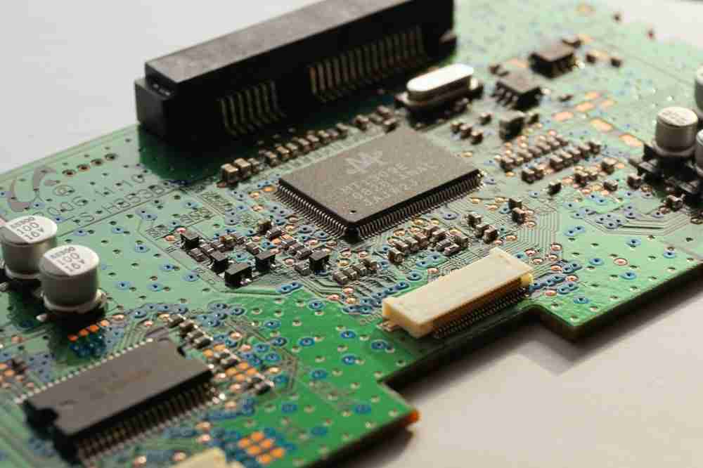
The increasing complexity of PCB forces the use of techniques that ensure increased utilization of PCB area, such as microholes with a diameter of 0.15mm or less. Blind and buried holes can also be used as microholes. The main advantage of these through-holes is that they can increase the interconnect density without increasing the number of layers or increasing the PCB size. This package density is sometimes required due to the EMC required to design equipment.
Electronic devices often have connectors that provide electrical connections to other device modules and allow for quick module replacement (for maintenance reasons, for example). If the connector is of poor heat resistance, it cannot be welded. They are assembled through a press assembly process. The process involves installing connectors by pressing them into dedicated through-holes with reduced diameter tolerances (standard values of ±0.05 mm). No specific design method is required for the pressing process; Nevertheless, the design engineer should ensure that the PCB manufacturer knows exactly which holes must be dedicated to press assembly.
processing
One of the non-standard machining methods for FR4 laminates is Z-wiring, which is milling specific areas of laminate to a specified depth. Z-wiring allows assembly of atypically tall parts, countersunk holes for countersunk screws, or installation of PCBS in non-standard (low) housing. When ordering PCBS that require Z-wire wiring, the PCB manufacturer must be provided with a clearly specified surface and depth of laminate machining. Note that the Z-path has its own machining tolerances, which are often similar to traditional milling. By default, Techno-Service uses a tolerance of ±50μm.
Another non-standard machining method is to metallize the edges of the PCB. Similar to through-holes, the edges can be electroplated to form a permanently reliable conductive layer. The solution is mainly used to improve the EMC of electronic equipment. The process is also used to build adapters between the main PCB and non-standard components (for example, later versions) or other PCBS that cannot be assembled by a standard process. In this case, the plating edge is made into a half hole reserved for downstream assembly. Another application of this process is its ability to customize edge joins.
Rely on quality to provide reliable PCB
Many electronic devices must provide high reliability. These requirements translate into high quality application components, assemblies, and PCBS. In this case, quality is defined by various industry standards, the most relevant of which is the IPC standard family (A-600, 6010, 6012, 6013, etc.). These documents provide a standardized and accepted standard for PCBS. These standards classify PCBS into performance (manufacturing) quality categories, taking into account a number of parameters: maximum hole coating thickness, minimum conductor width, dimensional tolerances, etc. Most PCB manufacturers set IPC class PCBS as secondary standards. Few PCB manufacturers include technical services that provide higher performance and quality PCBS: Class III. If the designer requires such a PCB, it should be indicated in the purchase order.


Just upload Gerber files, BOM files and design files, and the KINGFORD team will provide a complete quotation within 24h.