
Professional PCB manufacturing and assembly
Building 6, Zone 3, Yuekang Road,Bao'an District, Shenzhen, China
+86-13410863085Mon.-Sat.08:00-20:00

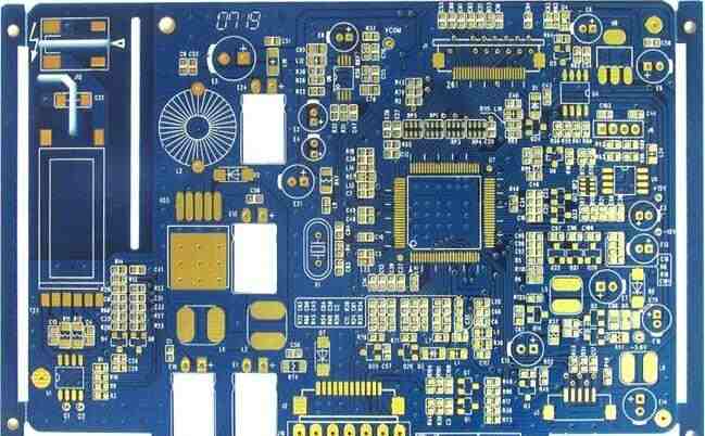
In PCB board design, the hole has four functions: electrical conduction, positioning, heat dissipation, convenient board division. And the hole is divided into through hole (PTH) and non-through hole (NPTH), and in the general design, only the PTH hole has a hole ring, NPTH hole is not equipped with a hole ring, but some special cases will also design the NPTH hole ring (at this time the hole ring plays a grounding role). The PTH metallized hole is conductive to the connected layer and has an electrical connection. The opposite is NPTH nonmetallic hole, refers to the hole inside without copper, electrical partition. NPTH non - sunk copper hole, hole wall without copper, generally is the positioning hole and gong wire hole. Dry film can be used to seal holes or in the pre - plating colloidal plug or after plating secondary drilling.
Use of PTH hole and NPTH hole:
PTH holes are metallized holes. Generally, PTH holes on circuit boards have two uses. One is used to weld the feet of traditional dip parts.
Another relatively small PTH, usually called via (through hole), is used to connect and connect the copper foil line between two or more layers of printed circuit board, because PCB is composed of a lot of copper layers piled up, each layer of copper (copper) will be paved with a layer of insulation layer, that is to say, copper layers can not communicate with each other, The connection of its signal is via, which is why it is called (conduction hole) in Chinese.
NPTH is nonmetallic hole, there is no copper inside the hole, electrical partition through the hole refers to the top and bottom of PCB board, similar holes and blind holes and buried holes, and through the hole can be PTH, can also be NPTH, according to the specific needs. For example, holes for connecting wires require PTH, and holes for fixing functions, such as screws, may be NPTH.
Function of PTH: On the non-conductive cell wall substrate of borehole, a thin layer of chemical copper is deposited as the substrate for subsequent copper plating. PTH process decomposition: basic degreasing →2 or 3 countercurrent washing → coarsing (micro-etching) → secondary countercurrent washing → preimpregnation → activation → secondary countercurrent washing → desviscosification → secondary countercurrent washing → sinking → secondary countercurrent washing → pickling.
PTH process description:
Alkaline degreasing: Remove oil, fingerprints, oxides, and dust from the surface of the plate. Then the pore wall is charged from negative adjustment to positive charge to promote the adsorption of colloidal palladium in the subsequent process. After degreasing, cleaning should be done in strict accordance with the guidelines and should be tested using a copper backlight test.
Microetching: Remove oxides from the surface of the circuit board and roughen the surface to ensure a good bond between the subsequent copper layer and the substrate bottom copper. The new copper surface has strong activity and can adsorb colloid palladium well.
Preimpregnation: mainly protects palladium tank from pollution of pretreatment tank, prolonging the service life of palladium tank. Except for palladium chloride, the main composition is the same as palladium can. Palladium chloride can effectively wet the pore wall and promote the activation solution to be activated into pores later, which is effective enough for activation.
Activation: After the polarity adjustment of pretreatment alkaline degreasing, the positively charged pore wall can effectively adsorb the negatively charged colloidal palladium particles to ensure the average, continuous and dense sinking of subsequent copper. Activation is crucial to the quality of subsequent copper tanks.
Control point: Specified time, standard stannous and chloride ion concentrations, specific gravity, acidity and temperature are also important and must be controlled in strict accordance with the operating instructions.
Peptidization: removal of stannous ions from colloidal palladium particles and exposure of palladium nuclei in colloidal palladium particles to directly catalyze initiation of chemical copper precipitation reactions. Experience shows that it is better to use fluoborate as desviscosifier.
Electroless copper plating: The autocatalytic reaction of electroless copper plating is caused by the activation of palladium nuclei, and both the new chemical copper and the reaction by-product hydrogen can be used as reaction catalysts for the catalytic reaction, allowing the copper precipitation reaction to continue. After this step, a layer of chemical copper can be deposited on the surface of the plate or on the wall of the hole. During this process, the bath should be kept under normal air agitation to convert more soluble bivalent copper.
The core function of PTH is to realize the conduction between layers of PCB circuit board by plating copper in the hole wall. It is the key point that double panel and multilayer board can play a role. The hole metalization technology is not complicated, and it can be simply divided into two parts: preparation for copper plating and copper plating. The quality of copper plating depends largely on the preparation of copper plating. As a result, people in the industry tend to focus on the reliability of PCB, to the preparation of copper plating part. At present, the industry mainstream preparation process for copper plating, there are three main: sinking copper, black hole, black shadow. (There are colloidal palladium, metal grouting, but not the current mainstream)
Copper deposition, also known as chemical copper deposition, its main principle is to use the displacement reaction in chemistry, deposit a layer of copper on the pore wall, as a conductive lead for subsequent copper plating. If it is conventional copper, its thickness is generally about 0.5μm. As the most traditional preparation process for copper plating, it has the following advantages and disadvantages:
1 Metal copper has excellent electrical conductivity (wire inside, the conventional use of copper wire as conductive).
2. The thickness can be adjusted in a wide range, wide adaptability (the lowest in the industry is about 0.3μm, the highest can be 30μm, directly replace the subsequent copper plating process).
3. The process is mature and stable, which can be applied to all types of circuit board products (PCB/FPC/RFPCB/ carrier board/metal substrate/ceramic substrate, etc.).

Disadvantages:
1. Formaldehyde is harmful to the health of operators.
2. Large investment in equipment, high production cost and environmental pollution.
3. The prescription control is short, and the effective time is generally 3-6 hours.
Black hole is a kind of direct electroplating technology. Its main principle is to use physical principle to adsorb carbon powder on the surface of the hole wall to form a conductive layer, which can be used as conductive lead for subsequent copper plating. Usually, the thickness is 0.5~1μm. As one of the current mainstream copper plating preparation processes, it has the following advantages and disadvantages:
1. No formaldehyde, small impact on the health of operators, and small pollution to the environment.
2. The equipment investment is small, the waste treatment is simpler, and the process cost is lower than that of copper sinking.
3. The potion and process are relatively reduced, the timeliness can reach 48H, and it is easier to maintain and manage.
Disadvantages:
1. In terms of conductivity, conductive toner is weaker than deposited copper layer.
2. Its applicability is not as wide as sinking copper, therefore, although it has been used on a large scale, but currently the industry is mainly used for dual panels, high-end products such as HDI board, almost not used.
Black shadow, strictly speaking, is a further development of black hole technology, its principle, advantages and disadvantages, are similar, and better than black hole. The main difference is that the conductive layer of the black hole is carbon powder, while the conductive layer of the black shadow is graphite. In addition, black holes are generally not used for high-end products, or with complex processes, but black shadow can, black shadow process has been partially replaced by sinking copper, widely used in high-end circuit boards, such as HDI board, IC carrier board, and sometimes even black shadow process is better than copper sinking process, such as selective graphic plating.
How to ensure safety in SMT patch processing
Feb 08,2023


Just upload Gerber files, BOM files and design files, and the KINGFORD team will provide a complete quotation within 24h.