
Professional PCB manufacturing and assembly
Building 6, Zone 3, Yuekang Road,Bao'an District, Shenzhen, China
+86-13410863085Mon.-Sat.08:00-20:00

Do you know all the six common sense introductions of PCB
Do you know that PCB manufacturers, PCB designers and PCBA manufacturers explain the six basic knowledge of PCB to you
Printed circuit boards, also known as printed circuit boards, are providers of electrical connections for electronic components.
Printed circuit board is usually represented by "PCB", not "PCB".
PCB design is mainly layout design; The main advantage of using circuit board is to greatly reduce wiring and assembly errors, and improve the automation level and production labor rate.
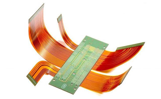
Printed circuit board can be divided into single panel, double panel, four layer board, six layer board and other multi-layer circuit boards according to the number of circuit board layers.
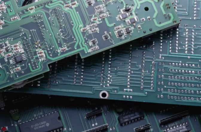
As PCB is not a general terminal product, the definition of its name is slightly confused. For example, the motherboard for personal computers is called the motherboard, but not the circuit board. Although there are circuit boards in the motherboard, they are not the same. Therefore, when evaluating the industry, they cannot be said to be the same. Another example: because there are integrated circuit parts loaded on the circuit board, the news media call it IC board, but in fact it is not the same as printed circuit board. The printed circuit board we usually refer to the bare board - that is, the circuit board without upper element devices.
Who invented PCB?
The creator of PCB was Paul Eisler, an Austrian. In 1936, he first used printed circuit boards in radios. In 1943, most Americans used this technology in military radios. In 1948, the United States officially recognized that this invention could be used for commercial purposes. Since the mid 1950s, PCB has been widely used.
Why is PCB green?
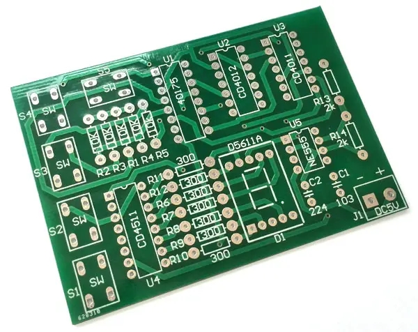
Careful, you may find that most PCBs are green (there are fewer PCBs in black, blue, red and other colors). Why? In fact, the circuit board itself is brown, and the green color we see is solder mask. The solder mask is not necessarily green, but red, yellow, blue, purple, black, etc., but green is the most common.
As for why green solder mask should be used, there are mainly the following statements:
1) Green is less irritating to eyes. The teacher told us that green is good for eyes, protects eyes and resists fatigue. It is not easy for production and maintenance personnel to have eye fatigue when staring at PCB for a long time, which is less harmful to the eyes.
2) Low cost. As green is the mainstream in the production process, the purchase volume of natural green paint will be larger, and the purchase cost of green paint will be lower than that of other colors. At the same time, using paint of the same color in mass production can also reduce the cost of changing lines.
3) When the board is welded in SMT, it needs to go through tin coating, pasting and final AOI verification. These processes all need optical positioning calibration. The green background is better for the identification of the instrument.
How is PCB designed?
To make a PCB, you must first carry out PCB layout design. PCB design needs to rely on EDA design software tools and platforms, such as Cadence Allegro, Mentor EE, Mentor Pads, Altium Designer, Protel, etc. At present, due to the continuous miniaturization, precision and high-speed of electronic products, PCB design should not only complete the circuit connection of various components, but also consider the challenges brought by high-speed and high-density.
The basic process of PCB design is: preliminary preparation → PCB structure design → PCB layout design → PCB constraint setting and wiring design → wiring optimization and silk screen placement → network DRC inspection and structure inspection → PCB board making.
What is the white print line on the PCB?
We often see white print lines on PCB. Have you ever thought about what they are? These white printing lines are actually used to mark components and print important PCB information on the board, which is called "screen printing". It can be screen printed on a board or printed on a PCB with an inkjet printer.
What are the components on PCB?
There are many separate components on the PCB, and each component has different functions, which together constitute the overall function of the PCB. Components on PCB include resistor, potentiometer, capacitor, inductor, relay, battery, fuse, transformer, diode, transistor, LED, switch, etc.
Is there any wire on the PCB?
Beginners may not know that PCB is actually connected without wires. This is interesting because most electrical equipment and technologies require wiring. There is no wire in PCB, but copper wire is used to lead the current to the whole equipment and connect all components.
Do you know that PCB manufacturers, PCB designers, and PCBA manufacturers explain the six basic knowledge of PCB to you.


Just upload Gerber files, BOM files and design files, and the KINGFORD team will provide a complete quotation within 24h.