
Professional PCB manufacturing and assembly
Building 6, Zone 3, Yuekang Road,Bao'an District, Shenzhen, China
+86-13410863085Mon.-Sat.08:00-20:00

The PCB industry also shows no signs of slowing down - the latest innovations help to address several challenges such as population aging and long-term disease management.
More and more, we see that the capabilities of new medical technologies push the limits of the design and manufacturing process. As devices and devices get smaller,
Its electronic components must also be smaller in size (with enhanced functionality).
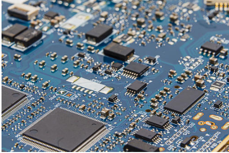
Due to the progress of technology, it is possible to produce smaller, denser, more reliable and more powerful PCB designs than before. In the past, most parts were designed using through-hole technology (THT). It is rarely found that the pin spacing of parts is less than 0.1 inch. Now, it is difficult to find parts that only use THT and have such a long pin spacing. For example, components such as micro BGA use previously unheard of pin to pin spacing.
Similarly, some discrete PCB components will disappear completely from the outer surface and be placed in the inner layer, which makes it possible to restore important areas of the outer surface. This is particularly common in resistors, which are now laminated to various internal layers using special materials in many high-density designs.
Looking ahead, 3D printing will further develop PCB by allowing the substrate to be printed layer by layer before adding liquid ink with electronic function on the top.
As a result of these advances, design has begun to play an increasingly important role in the field of health care in the areas of diagnosis, treatment, monitoring, etc. For a long time, PCB has been used in medical imaging systems such as CT, CAT and ultrasonic scanners, as well as computers used to compile and analyze images. Similarly, heart rate, blood pressure and blood glucose monitoring devices rely on PCB electronic components to obtain accurate readings.
Now, we also see that PCB is implanted or ingested in more and more internal medical devices (such as pacemakers, complex neural prostheses and gastrointestinal tracking devices). For example, a pill sized PCB camera composed of an image sensor, an aperture and a lens can be installed on the board. The patient can then swallow these ingredients to take digital images and videos of the digestive tract.
Medical PCB
When designing and developing these boards for medical PCBs, special attention must be paid to reliability, as failures may be critical to patient health. In many cases, PCBs must also meet strict hygiene standards, especially for implants.
Various additional steps, such as copper plating, surface metallization, and ink application, can help to produce reliable and repeatable boards. By shortening the circuit path, embedded components can usually improve the performance of high-speed circuits in PCB.
In order to further reduce the scale of medical technology, we are also beginning to see the trend of flexible electronic products. These next generation components are critical to creating complex devices that can fit into smaller physical spaces, such as those deployed in the human body.
Most devices achieve flexibility by patterning metals and semiconductors into flexible structures or by using malleable materials such as conductive polymers. Transistors and integrated PCB circuits can also be made of threads and used in conjunction with thread based sensors to create fully flexible multiplexing devices. These "soft electronic products" can then be woven into fabrics and worn on the skin, or (theoretically) implanted into the skin, heart and even brain through surgery.
Completely flexible electronic equipment can achieve a wide range of applications without affecting functions. For example, electronic medical tattoos and adhesive sensors can check vital signs and easily transmit results via Bluetooth. Similarly, smart contact lenses can be filled with thousands of biosensors, and can be carefully designed to obtain early indicators of cancer and other diseases.
Devices that can measure anything from people's pulse and heart rate variability to their blood pressure and respiratory rate are also taking full advantage of soft electronic devices. These types of PCB technologies have been helpful in diagnosis, enabling patients and medical practitioners to monitor the condition for a long time without regular testing.
So, this is what happened now. But what is the future of electronics in MedTech? About 150 years ago, people often died of diseases that can be easily treated (and prevented) today. However, the emergence of modern medicine has effectively doubled the average life span of human beings from 40 years old to 80 years old in more than a century.
Thanks to the latest development of PCB technology, we are likely to see technology in the medical field continue to extend our service life. After all, robotic prostheses are already in use, and robotic organs are currently being developed, such as an artificial pancreas that automatically dispenses drugs to control diabetes.


Just upload Gerber files, BOM files and design files, and the KINGFORD team will provide a complete quotation within 24h.