
Professional PCB manufacturing and assembly
Building 6, Zone 3, Yuekang Road,Bao'an District, Shenzhen, China
+86-13410863085Mon.-Sat.08:00-20:00


1、 Stacking of PCB proofing pads
1. The stacking of PCB pads (except the external bonding pads) means the stacking of holes. The drill bit is broken due to repeated drilling at the drilling union, resulting in hole damage.
2. Two holes in the multilayer board are stacked. For example, one hole position is a barrier disk, and the other hole position is a connecting disk (rosette pad). In this way, the negative film is shown as a barrier disk, and the composition is invalid.
2、 Misuse of graphic layer
Some useless connections have been made on some graphic layers, but the original four layer board has more than five layers of lines planned, which makes a misunderstanding.
2. In planning, we need to save energy. Take Protel software as an example, we use the Board layer to draw lines that are common to all layers, and also use the Board layer to draw marked lines. In this way, when photo drawing data, because the Board layer is not selected, the connection is missed and the circuit is broken, perhaps because the marked lines of the Board layer are selected, the circuit is short circuited. Therefore, we should adhere to the integrity and clarity of the graphic layer when planning.
3. It violates the conventional planning, for example, the component surface is planned at the bottom layer, and the welding surface is planned at the top, which is inconvenient.
3、 Random placement of characters
1. The SMD pad of the character cover pad brings inconvenience to the on-off inspection of the printed board and the welding of components.
2. Character planning is too small, which makes screen printing difficult, and too large makes characters stacked with each other and difficult to distinguish.
4、 Setting of PCB Proofing Single sided Pad Aperture
1. Single sided PCB pads generally do not drill holes. If the holes need to be marked, the hole diameter should be planned as zero. It is assumed that the numerical value is planned, so that when the drilling data occurs, this orientation presents the coordinates of the hole and presents a problem.
2. Single side pads such as drilled holes shall be specially marked.
5、 Draw pads with filler blocks
Pads drawn with filler blocks can pass DRC inspection during route planning, but processing is not allowed. Therefore, solder resistance data cannot be directly generated for such pads. When solder resistance is applied, the filler block area will be covered by solder resistance, resulting in difficulty in equipment welding.
6、 The electrical layer is both a mosaic pad and a connection
As the power source of the patterned bonding pad method is planned, the image on the stratum is opposite to that on the practical printed circuit board, and all connections are barrier lines, which should be very clear to planners. By the way, be careful when drawing several groups of power supplies or barriers of several fields, and do not leave gaps to short circuit the two groups of power supplies, nor form a closed area of the connection (to separate a group of power supplies).
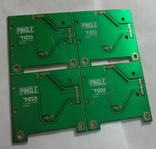
PCB proofing
7、 The definition of PCB proofing processing level is not clear
1. The single panel is planned on the TOP layer. If the positive and negative construction is not clarified, the fabricated board may be installed with equipment and not welded well.
2. For example, when planning a four ply board, four ply boards are selected, but they are not placed in this order during processing, which requires clarification.
8、 There are too many filler blocks in the planning or the filler blocks are filled with very thin lines
1. The photo data is lost and incomplete.
2. Because fill blocks are drawn one by one with lines during photo data processing, the amount of photo data generated is appropriately large, which adds difficulty to data processing.
9、 The bonding pad of surface mounting equipment is too short
This is for on-off inspection. For too dense surface mounted equipment, the spacing between its two feet is appropriate small, and the pad is appropriate thin. It is necessary to staggered the up and down (left and right) directions of the equipment inspection needle. If the pad is too short, although it does not affect the equipment, the inspection needle will not be staggered.
10、 Spacing between large grids is too small
The edge between large area grid lines and the same line is too small (less than 0.3mm). During the manufacturing process of printed circuit board, many broken films are attached to the board after the development of the image.
11、 Large area copper foil is too close to the outer frame
The distance between the large area copper foil and the outer frame shall be at least 0.2mm, because milling to the copper foil during shape milling will simply cause the problem of copper foil warping and solder resistance falling.
12、 Unclear outline border planning
Some customers have planned the contour lines in waiting, and these contour lines do not coincide. It is difficult for PCB manufacturers to determine which contour line should prevail.
13、 Uneven graphic planning
When conducting pattern electroplating, the coating is uneven, which affects the quality.


Just upload Gerber files, BOM files and design files, and the KINGFORD team will provide a complete quotation within 24h.