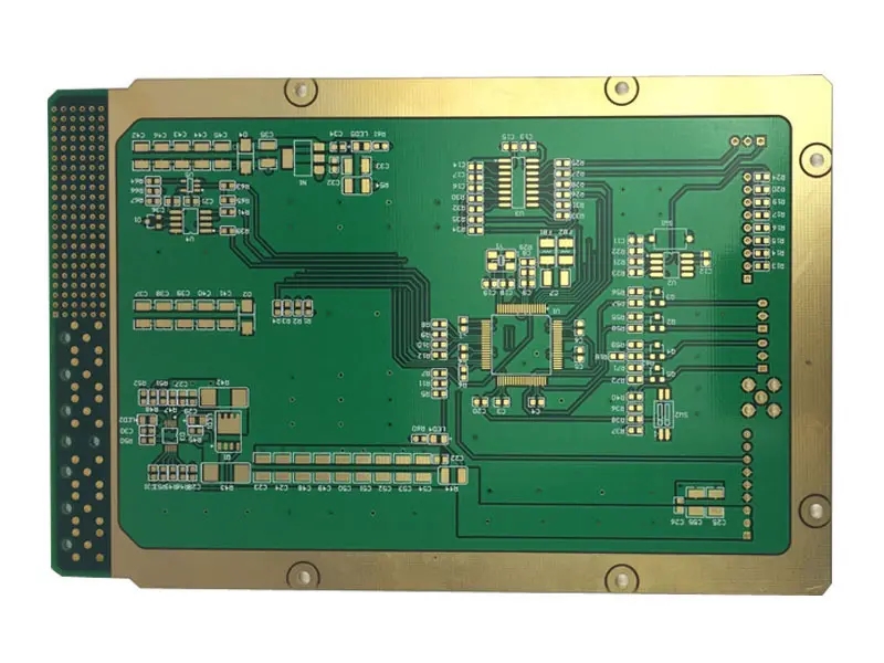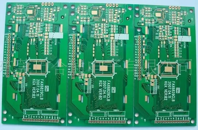
PCB moves towards high-density and refined products, which attract the most attention
At present, PCB products begin to move from traditional HDI/BUM boards to high-density HDI/BUM boards, IC packaging base (carrier) boards, embedded component boards, and rigid flexible boards. PCB will eventually reach the "limit" of "printed circuit boards". Finally, it will inevitably lead to a "qualitative change" from "electrical transmission signals" to "optical transmission signals", and replace printed circuit boards with printed optical circuit boards.
Due to the rapid development of miniaturization, high-performance, multi-function and high frequency (fast) signal transmission of electronic products, PCB must rapidly move from the traditional PCB industry to the product development characterized by high density and refinement. PCB products have begun, partially or comprehensively moving towards HDI/BUM boards, packaging base (carrier) boards, integrated (embedded) component printed boards (ICPCB) and rigid flexible printed boards (G-FPCB). In the future, these four types of PCB products will certainly become the four highlights of the PCB industry. In the future, more advanced printed optical circuit boards that transmit and calculate with "optical signal" will also replace the current printed circuit boards that transmit and calculate with "electrical signal".
HDI/BUM board core board output value accounts for 95%
HDI/BUM board is a kind of PCB with higher density than conventional printed boards. It can be divided into HDI/BUM boards with "core board" and HDI/BUM boards without "core board".
HDI/BUM board with "core board" is a PCB formed by several higher density interconnection "layers" on the "product" of one side or both sides of "conventional printed board". In fact, HDI/BUM board with core board is a structural form of "transition" from "conventional printed board" to higher density PCB to meet the requirements of very high density installation. At the same time, no matter from equipment, process technology and management, it is also the best way to better adapt to the transition from the original PCB industry to the very high density PCB products. If the existing PCB production equipment, testing and technology can be improved a little, then development and production can be carried out. The investment is small, the cost is low, and the management and production have good continuity and scalability, which is accepted by most PCB manufacturers. Therefore, HDI/BUM boards with core boards account for about 95% of the current HDI/BUM board output value.
HDI/BUM board with core board, its high-density improvement is significant and outstanding, such as the use of 4+12+4 200 × Compared with 400, the HDI/BUM board of 300cm2 × 450 cm2 46 layer buried/blind hole high rise board has higher capacity, better electrical performance, reliability and service life.
At present, most HDI/BUM boards without "core board" use conductive adhesive technology, which has limited scope of use, so the proportion is very small.
IC packaging substrate is the most important to solve CTE matching problem
IC packaging substrate is developed on the basis of HDI/BUM board by continuing to "deepen (high-density)", or IC packaging substrate is HDI/BUM board with higher density. In essence, the primary problem of IC packaging substrate is the matching (compatibility) of CTE (coefficient of thermal expansion) with the packaging element (assembly) to be packaged, followed by the high-density problem.

In essence, PCB provides interconnection and mechanical (physical) support for elements (assemblies). In today's electronic packaging market, there are mainly three types of packaging: (1) organic substrate packaging; (2) Ceramic substrate packaging; (3) Ideal size and speed (i.e. chip level) packages, such as Wafer Level Package (WLP) and Direct Die Attach (DDA). Obviously, conventional PCBs do not have the capability of these advanced packaging (low CTE occasions). Therefore, the PCB industry must develop technologies and products that can carry out these advanced packaging substrate materials.
CTE matching (compatibility) between packaging substrate and packaging element (assembly). When the CTE of the two do not match or differ greatly, the internal stress generated after welding and packaging will threaten the reliability and life of electronic products. Therefore, the problem of CTE matching (compatibility) between the packaged substrate and the packaged elements (assemblies) requires that the CTE difference between the two become smaller and smaller with the high-density installation and the reduction of the area of solder joints.
IC packaging substrate is mainly embodied in:
1. The CTE of the substrate material is smaller or matched, that is, the CTE of such IC substrate must be significantly reduced and close to (compatible with) the CTE of the chip pin to ensure reliability;
2. It is directly used for packaging of bare chips (KGD), so higher density of IC substrate is required;
3. The thickness of the packaging substrate is thin and the size is very small, most of which are less than 70mm × 70mm;
4. Thin low CTE base materials are mostly selected, such as PI materials, ultra-thin glass fiber cloth and carbon fiber CCL materials.
The way out is to embed active and passive components in integrated component PCB at the same time
With the development and progress of high-density electronic products, high-frequency signal transmission and high-speed digitization, the number of I/O chips and the number of passive components have increased rapidly, which has increasingly affected the reliability of electronic products and the integrity of transmission signals. The way out is to move towards integrated (embedded) component printed boards.
Development steps: integrated (embedded) passive components (mainly capacitors, resistors and inductors) → integrated (embedded) active components (IC modules).
1. Embedded passive components
The number of passive components increases rapidly. The number of passive components will increase rapidly with the increase of IC module integration (or I/O number), high frequency signal transmission and high-speed digitization (the assembled active components/passive components will change from 1 ∶ 10 - → 1 ∶ 20 - → 1 ∶ 30 - → 1 ∶ 50): the passive components account for more and more board areas (30% → 40% → 50% → 70%), which affects high-density; The number of welding points of passive components is also increasing, which affects the reliability of connection, because welding points are one of the main failures of electronic products. The ratio of the number of various elements (groups) for conventional assembly is shown in the table.
The increase of passive components will inevitably bring problems. With the increase of passive components, there are more and more solder joints, and the welding reliability is lower and lower. The solder joints have always been the largest failure rate of electronic products; The electromagnetic interference caused by the loop formed by passive components is becoming more and more serious; The increase of passive components increases the size (area) of the board, which has a negative impact on the performance of high-frequency and high-speed digital transmission.
Embedded passive components can eliminate these effects and significantly improve the integrity and reliability of the transmission signal.
The embedded passive components can be divided into: embedded single passive components; Embedded "integrated" (combining capacitors, resistors, etc.) passive components.
2. Embedded active components.
While embedding passive components, it is also embedding active components (various IC components). It is in the process of development and trial, which is the road of future development.
The growth rate of rigid flexible printed boards will be accelerated in the future
There are many advantages of rigid flexible printed boards, but the main ones are: improving the reliability of high-density connections (replacing mechanical connectors, etc.); It is conducive to miniaturization; Installation flexibility (bending or folding) and implementation of three-dimensional (3D) assembly; Simplify the installation process and maintenance; The post-processing is convenient, which has obvious advantages. Therefore, it will develop with the development of miniaturization, high-performance and multi-function of electronic products.


