
Professional PCB manufacturing and assembly
Building 6, Zone 3, Yuekang Road,Bao'an District, Shenzhen, China
+86-13410863085Mon.-Sat.08:00-20:00

PCB innovation is the driving force for the sustainable development of PCB industry
Printed circuit board (PCB) has become an indispensable part of modern electronic equipment. No matter the high-end electronic equipment in the world, or the household appliances and electronic toys, there is no shortage of PCB carrying electronic components and electrical signals, and PCB is developing with the development of the entire electronic information industry.
The innovation of printed circuit lies first in the innovation of PCB products and markets. The earliest PCB product was a single panel, with only one layer of conductor on the insulating board, and the line width was measured in millimeters. It was commercially applied to semiconductor (transistor) radios. Later, with the advent of televisions, computers, etc., PCB products have been innovated. Double sided boards and multilayer boards have emerged. There are two or more layers of conductors on the insulation board, and the circuit width has gradually decreased. In order to adapt to the miniaturization and lightweight development of electronic equipment, flexible PCB and rigid flex PCB have emerged.
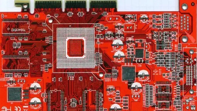
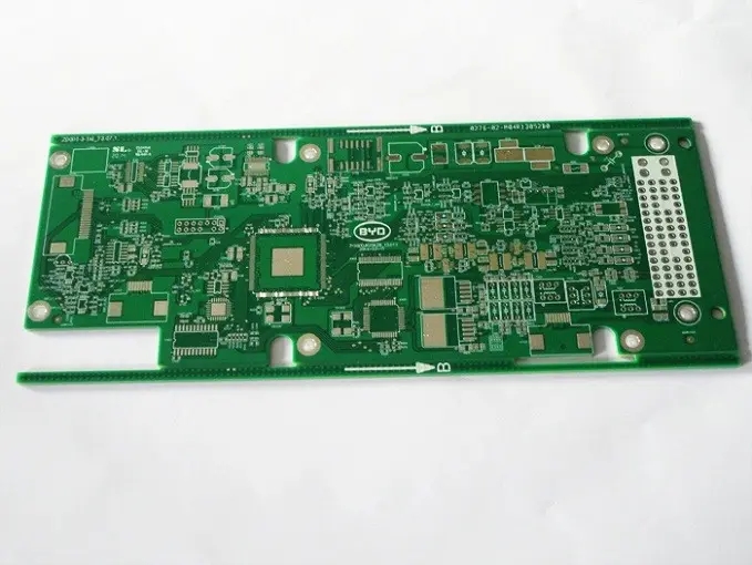
At present, the main markets of PCB are computers (computers and peripherals), communication equipment (base stations and handheld terminals, etc.), home electronics (televisions, cameras, game consoles, etc.), automotive electronics, etc. PCB products are mainly multilayer boards and high-density interconnection (HDI) boards. With the development of computers toward high speed and large capacity, mobile phones toward multi-function intelligence, televisions toward high-definition 3D, and automobiles toward high security intelligence, HDI printed boards have also changed from wire connection functions to electronic circuit functions, that is, in addition to the basic conductor lines, PCB products also include passive components such as resistors, capacitors, and active components such as IC chips. The new generation HDI printed board is the embedded component printed board with components inside. In order to adapt to high frequency and high-speed signal transmission applications, the newer generation of printed boards will contain optical fibers and waveguides between PCB layers to form photoelectric printed boards suitable for signal transmission above 40GHz.
It is precisely because of the continuous innovation of PCB products that we have ushered in one spring after another for the development of printed circuits. Intelligent mobile phones will bring the climax of embedded component printed boards, LED energy-saving lighting will bring the climax of metal based printed boards, and e-books and film displays will bring the climax of flexible circuit boards.
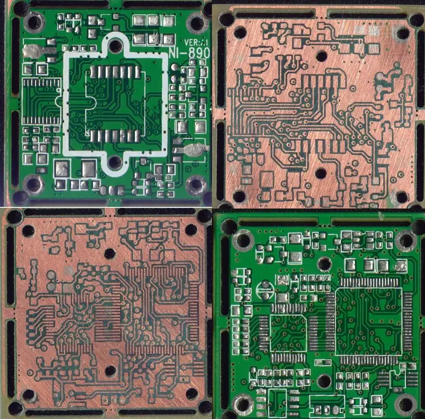
The innovation of printed circuit is based on technological innovation. The traditional technology of PCB manufacturing is copper foil etching (subtractive method), that is, the unwanted copper layer is removed by etching the copper clad insulating substrate with chemical solution, leaving the required copper conductor to form a circuit pattern; For double-sided and multilayer boards, the interlayer interconnection is conducted by drilling and electroplating copper. Now this traditional process has been difficult to adapt to the production of micro HDI thin circuit boards, to achieve rapid and low-cost production, and to achieve the purpose of energy conservation, emission reduction and green production. Only technological innovation can change this situation.


Just upload Gerber files, BOM files and design files, and the KINGFORD team will provide a complete quotation within 24h.