
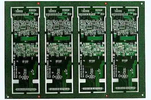
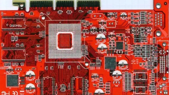
Professional PCB manufacturing and assembly
Building 6, Zone 3, Yuekang Road,Bao'an District, Shenzhen, China
+86-13410863085Mon.-Sat.08:00-20:00

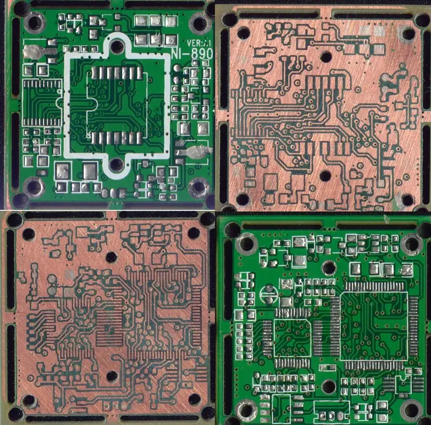
Electronic manufacturers explain the significance of the "layer" of pcb manufacturing
1 Signal layer
The signal layer is mainly used to arrange the wires on the circuit board. Protel 99 SE provides 32 signal layers, including Top layer, Bottom layer and 30 MidLayers.
2 Internal plane layer
Protel 99 SE provides 16 internal power supply layers/grounding layers. This type of layer is only used for multilayer boards, mainly for laying power lines and grounding wires. We call it double-layer board, four layer board, and six layer board, generally referring to the number of signal layers and internal power supply/grounding layers.
3 Mechanical layer
Protel 99 SE provides 16 mechanical layers, which are generally used to set the overall dimensions, data marks, alignment marks, assembly instructions and other mechanical information of the circuit board. The information varies according to the requirements of the design company or PCB manufacturer. Execute the menu command Design | MechanicalLayer to set more mechanical layers for the circuit board. In addition, the mechanical layer can be attached to other layers to output and display together.
4 Solder mask layer
Apply a layer of paint, such as solder mask, on all parts outside the bonding pad to prevent tin coating on these parts. The solder mask is automatically generated for matching pads during the design process. Protel 99 SE provides two solder mask layers: Top Solder and Bottom Solder.
5 Paste mask layer
Its function is similar to that of the solder mask, but the difference is that the pad of the corresponding surface bonded component is welded by the machine. Protel99 SE provides two solder paste protective layers: Top Paste (top layer) and Bottom Paste (bottom layer).
Mainly for SMD components on PCB. If all the boards are placed with Dip (through hole) components, Gerber files do not need to be output for this layer. Before pasting SMD components onto PCB, solder paste must be coated on each SMD pad. The steel mesh for tin coating must need this Paste Mask file before film can be processed.
The most important thing to be clear about Gerber output of Paste Mask layer is that this layer is mainly for SMD components. At the same time, compare this layer with the Solder Mask introduced above to find out the different functions of the two layers, because the two film images are very similar from the film image.
6 Keep out layer
It is used to define the area where components and wiring can be effectively placed on the circuit board. Draw a closed area on this layer as the valid routing area. You cannot automatically layout and route outside this area.
7 Silkscreen layer
The silk screen layer is mainly used to place printed information, such as outline and annotation of components, various annotation characters, etc. Protel 99 SE provides two silk screen layers: Top Overlay and Bottom Overlay. Generally, all marking characters are on the top screen layer, and the bottom screen layer can be closed.
8 Multi layer
Pads and through-hole on the circuit board need to penetrate the whole circuit board to establish electrical connection with different conductive graphic layers. Therefore, the system has set up an abstract layer - multilayer. Generally, pads and vias must be set on multiple layers. If this layer is closed, pads and vias cannot be displayed.
9 Drill layer
The drilling layer provides the drilling information during the manufacturing process of the circuit board (such as the pad, through hole drilling is required). Protel 99 SE provides two drilling layers, namely, Drillgrid and Drill drawing.
PCB manufacturing, PCB design and PCBA processing manufacturers explain the meaning of the "layer" of pcb manufacturing.


Just upload Gerber files, BOM files and design files, and the KINGFORD team will provide a complete quotation within 24h.