
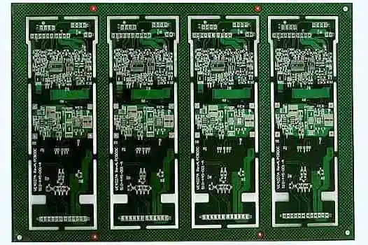
Professional PCB manufacturing and assembly
Building 6, Zone 3, Yuekang Road,Bao'an District, Shenzhen, China
+86-13410863085Mon.-Sat.08:00-20:00

Circuit board manufacturer: explanation of solder mask and soldering aid
Solder mask
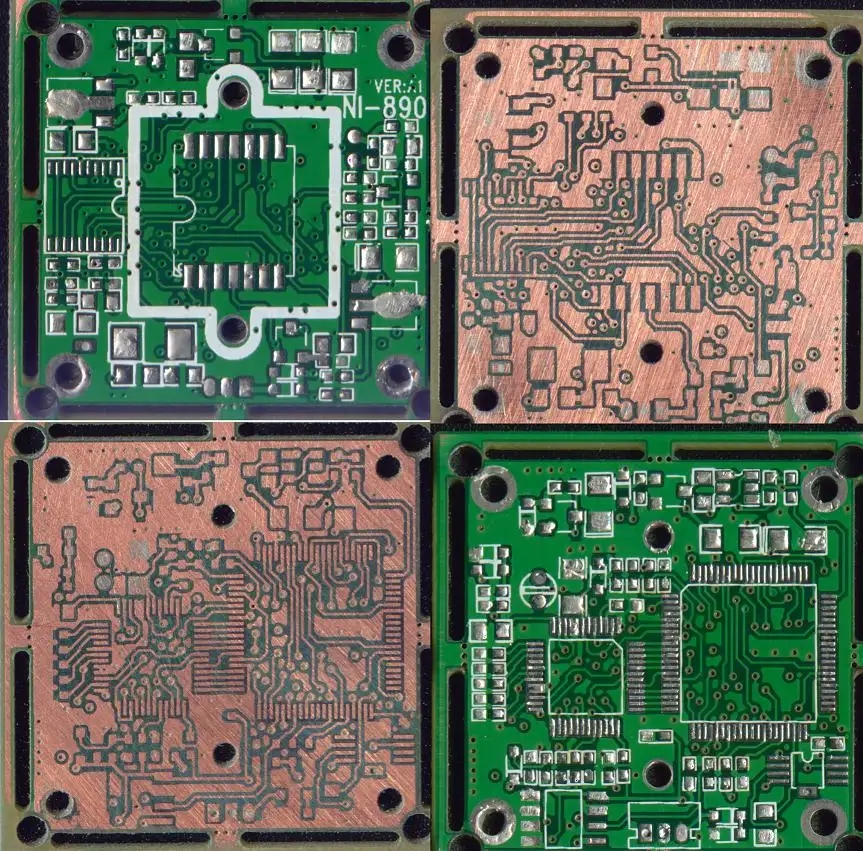
Solder mask refers to the part on the board to be coated with green oil; Because it is a negative output, the actual effect of some solders mask is not green, but tinned, silver white!
Welding flux
The paste mask is used when the machine is mounted. It corresponds to the bonding pads of all mounting elements. The size is the same as that of the toplayer/bottomlayer layer. It is used to open the tin leakage of the steel mesh.
The two layers are used for tin coating and welding, not one for tin coating and one for green oil coating; Is there a layer that is covered with green oil? As long as there is a layer on an area, it means that the area is covered with insulating green oil? I haven't met such a layer yet! By default, the pads on the PCB we drew all have a solder layer, so the pads on the PCB we made are coated with silver solder, which is not surprising; However, the wiring part on the PCB we drew only has the top layer or bottom layer layer, and no solver layer. However, the wiring part on the PCB made is covered with a layer of green oil.
It can be understood as follows:
1. Welding resistance layer means to open a window on the whole piece of welding resistance green oil, so as to allow welding!
2. By default, areas without solder mask should be painted green!
3. The paste mask layer is used for chip packaging! SMT encapsulation uses: the toplayer layer, the topsolver layer, and the toppaste layer. The toplayer is the same size as the toppaste, and the topsolver is one circle larger than them. DIP encapsulation only uses: topsolder and multilayer layers (after a bit of decomposition, I found that the multilayer layer is actually the top layer, bottomlayer, topsolder, and bottomlayer layers with overlapping sizes), and the top layer/bottomlayer is one circle larger than the top layer/bottomlayer.
Question: Is it correct to say that the copper skin corresponding to the solder layer can only be tinned or gold-plated if there is copper? This sentence was said by a person working in a PCB factory, which means that if the part of the painting on the solder layer is made of tin, the corresponding solder layer part must have a copper sheet (that is, the area corresponding to the solder layer must have the top layer or bottom layer part)! Now: I come to a conclusion: "The copper skin corresponding to the solder layer can only be tinned or gold-plated if it has copper" is correct! The solder layer represents the area not covered with green oil!
The circuit board manufacturer, circuit board designer and PCBA processor will explain the solder mask and soldering aid layer.


Just upload Gerber files, BOM files and design files, and the KINGFORD team will provide a complete quotation within 24h.