
Professional PCB manufacturing and assembly
Building 6, Zone 3, Yuekang Road,Bao'an District, Shenzhen, China
+86-13410863085Mon.-Sat.08:00-20:00


Q&A on common PCB design knowledge
Q1: What is a part package and what is the difference between it and a part?
(1) Part packaging refers to the appearance and solver spot position indicated when the actual part is welded to the PCB
(2) Part packaging is only part appearance and solver spot position; On the other hand, the same parts can also have different packaging, such as RES2, which represents resistance, in the packaging form of AXAIL0.4., AXAIL0.3., AXAIL0.6, and so on. In this regard, when acquiring welded parts, we should not only know the name of the part, but also know the packaging of the part
(3) The package of parts can be specified in the design of the circuit diagram When designing a circuit diagram, you can specify schematic settings in the Part Properties dialog box, or you can specify a part package when importing a network table
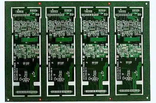
PCB board

Q2: Wires, cables and networks?
Metal wire, also known as copper film wire, short circuit wire, is used to connect each solder joint. It is a printed circuit board. The design of the printed circuit board is about how to arrange wires Another type of conductor associated with a conductor, usually called a flying wire or pre drawn wire After the network table is introduced, the system generates it according to the rules to guide the wire routing There is an essential difference between flying wire and conductor The flying wire is only a form of connection, which is only a form of connection between solder joints. It has no meaning for electric connection Arrange the wires according to the connection relationship between the solder joints instructed by the flying wire, which is a connecting wire with electrical connection significance The network is different from the wire, which also includes the solder joint. In addition, the network includes not only the wire, but also the solder joint connected to the wire
Q3: What is the difference between an inner layer and a middle layer?
The middle layer and the inner layer are two concepts that are easily confused The middle layer refers to the middle layer used for wiring, which is distributed in the conductor; The inner layer refers to the power layer or ground layer, which is usually composed of a whole piece of copper film without wiring
Q4: What are internal network tables and external network tables, and what are the differences between them?
The network table is divided into external network table and internal network table. The external network table represents the network table, that is, the schematic network table generated by Sch or other schematic design software; The internal network table is based on the imported external network table, which is modified and used for PCB system wiring. Strictly speaking, these two Nettables are completely different concepts, but readers do not need to strictly distinguish them.
Q5: What does Net manager do?
First, introduce the network table. The introduction of the network table is actually the process of loading schematic design data into the PCB of the PCB design system All data changes in the PCB design system can be completed by using the netlist macro, which is automatically generated by comparing and analyzing the netlist file with the internal data of the PCB system Secondly, the network table manager can be used to directly edit the connection relationship between each component of the circuit board in the PCB system to form a network table
Q6: What is a classroom? What are the benefits of introducing classroom concepts?
A class is a collection of units with the same meaning. Class definitions in PCB are open to users, who can define the meaning and composition of classes themselves. There are two main purposes to introduce classes into PCB: (1) Convenient wiring F In the wiring process of the circuit board, some networks need special processing, such as some important data lines. In order to avoid interference from other components on the circuit board, a safe distance between these data lines and other components often needs to be added in the wiring process. These data lines can be divided into one class, which can be added to the rules when setting automatic routing safety spacing rules, and the safety spacing can be added appropriately. In addition, the safety spacing of all data lines in this class will be added during automatic routing; Power and grounding cables shall be thickened to ensure the reliability of connection. Power and ground cables can be classified into one category. When setting width constraint rules, you can add this category to the rules and add wire widths appropriately. This type of power cord and ground wire will be wider.
(2) Easy to manage circuit board component F For a large circuit board, it has many parts packaged, thousands of networks, and is very messy. Using classes can easily manage circuit boards. For example, to classify all input networks in a circuit board, you only need to view this input network class when searching for input networks. Circuit boards can also be classified by limited voltage resistance. When searching for voltage limiting resistance, you only need to view this voltage limiting resistance category.
Question 7: How do I add additional solder joints to the network?
You can first add the solder joint to the circuit board, and then press the solder joint twice to open the "Solder Joint Property Setting" dialog box. Select the appropriate network in the Advanced Net items, and you can complete the placement of the solder joint
Q8: What is the use of internal segmentation?
The inner layer can be used to connect some important circuits. It can improve the anti-interference ability and protect important circuits
Q9: What is the impact of copper cladding and what should be paid attention to?
The main function of copper plating is to improve the anti-interference ability of the circuit board If you want to wrap the wire or fill the tear drop on the wire, then it should be on the pcb


Just upload Gerber files, BOM files and design files, and the KINGFORD team will provide a complete quotation within 24h.