
Professional PCB manufacturing and assembly
Building 6, Zone 3, Yuekang Road,Bao'an District, Shenzhen, China
+86-13410863085Mon.-Sat.08:00-20:00

Partitioning Design of PCB Mixed Signal
For PCB, how to reduce the interference between digital and analog signals? Two basic principles of electromagnetic compatibility (EMC) must be understood before design: the first principle is to minimize the current loop area; The second principle is that the system uses only one reference plane. On the contrary, if the system has two reference planes, it is possible to form a small particle antenna (note: the radiation of a small particle antenna is significant to the length of the line, current, and the frequency) If the signal does not return through the smallest possible loop, a large circular antenna can be formed Avoid both as much as possible in your design
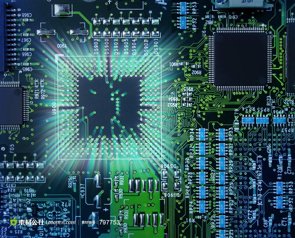
PCB board

It is recommended to separate digital grounding and analog grounding on the mixed signal circuit board to achieve isolation between digital grounding and analog grounding Although this method is feasible, it has many potential problems, especially in large complex systems The key problem is not to wire across gaps. Once wiring across gaps, electromagnetic radiation and signal crosstalk will increase dramatically The common problem in PCB design is the electromagnetic interference caused by the signal line passing through the ground or power supply We use the above segmentation method. The signal line crosses the gap between two grounding wires. What is the return path of the signal current? Replace the two partitioned lands are connected at some point (usually a single point at one point) The high frequency current flowing through the large loop will generate radiation and high grounding inductance If the low level analog current flowing through the large loop is easy to be interfered by external signals Unfortunately, when these parts are connected together at the power supply, a very large current loop is formed In addition, analog and digital dipole antennas are formed by connecting long wires
Understanding the path and mode of current return to ground is the key to optimize the design of mixed signal circuit board. Many design engineers only consider the flow direction of the signal current, ignoring the specific path of the current. If the ground floor must be partitioned and must be routed through the gap between partitions, a single point connection can be made between the partitioned floors to form a connection bridge between the two ground floors, and then routed through the connection bridge. In this way, a DC return path can be provided below each signal line to form a smaller loop area.
Optical isolation devices or transformers can also be used to enable signals to pass through the division gap. For the former, it is the light signal that spans the gap between partitions. In the case of transformers, it is the magnetic field that crosses the gap between the diaphragms. Differential signals can also be used: signals flow in from one line and return from another, in which case they are used unnecessarily as a return path.
In order to explore the interference of digital signals to analog signals, we must first understand the characteristics of high-frequency current. High frequency current always selects impedance (inductance), that is, the path directly below the signal. This return current will flow through the adjacent circuit layer, regardless of whether the adjacent layer is the power layer or the ground layer. In practice, it is usually preferred to divide PCB evenly into analog and digital parts. The analog signal is routed in the analog area of all layers of the circuit board, while the digital signal is routed in the digital circuit area. In this case, the digital signal return current will not flow into the ground of the analog signal. Only when the digital signal passes through the digital part of the circuit board or the analog signal passes through the digital part of the circuit board will the interference from the digital signal to the analog signal occur. This problem is not due to the lack of segmentation, but the real reason is the improper wiring of digital signals.
PCB design adopts a unified pipeline. Through the division of digital circuit and analog circuit and proper signal wiring, it can usually solve some difficult layout and wiring problems, and there are no potential problems caused by grounding segmentation. In this case, the layout and partitioning of components are critical to determining design quality. If the layout is correct, the digital ground current will be limited to the digital part of the circuit board and will not interfere with the analog signal. Such wiring must be carefully checked to ensure full compliance with the wiring rules. Otherwise, the incorrect signal line will completely destroy the very good circuit board.
When replacing A/ When the analog and digital grounding pins of the D converter are connected together, most A/D converter manufacturers recommend using short leads to connect AGND and DGND pins to the same low impedance grounding (note: since analog and digital grounding are not connected together inside most A/D converter chips, analog and digital grounding must be connected through external pins), Any external impedance connected to the DGND will couple more digital noise to analog circuits inside the IC through parasitic capacitors. According to the suggestion, both AGND and DGND pins of A/D converter need to be connected to analog ground, but this method raises some problems, such as whether the ground terminal of digital signal decoupling capacitor should be connected to analog ground or digital ground.
If the system has only one A/D converter, the above problems can be easily solved. The grounding is divided, and the analog and digital grounding parts are connected together under the A/D converter. When using this method, it must be ensured that the bridge width between the two websites is equal to the IC width, and no signal line can pass through the partition gap. If the system has multiple A/D converters, such as 10 A/D converters, how to connect them? If analog and digital grounding are connected under each A/D converter, multipoint connection will be generated, and isolation between analog and digital grounding will be meaningless. Failure to do so violates the manufacturer's requirements. To do this, you must first put on your uniform. As shown in Figure 4, grounding is evenly divided into analog and digital parts. This layout not only meets the requirements of IC device manufacturers for low impedance connection of analog and digital grounding pins, but also avoids the electromagnetic compatibility problems caused by loop antennas or dipole antennas.
If you have questions about the unified method of mixed signal PCB design, you can use the ground plane division method to lay out and route the entire circuit board. In the design, attention should be paid to making the circuit board easy to connect with the jumper or 0 ohm resistance. In future experiments, the spacing should be less than 1/2 inch. Pay attention to zoning and wiring to ensure that there is no digital signal line above the analog part on all layers, and there is no analog signal line above the digital part. In addition, no signal wire shall pass through the grounding gap or the gap between the split power supplies. To test the function and EMC performance of the circuit board, connect the two floors together through a 0 ohm resistor or jumper, and retest the function and EMC performance of the circuit board. The comparison test results show that, compared with the folding solution, the unified solution is superior to the folding solution in terms of function and EMC performance in almost all cases.
Is the method of land division still effective?
This method can be used in three situations: some medical devices need to be connected to the patient's circuit and the system with very low leakage current; The output of some industrial process control equipment may be connected to noise and high-power electromechanical equipment; Another case is that PCB layout is subject to specific restrictions. The mixed signal PCB usually has a separate digital and analog power supply, which can and should have a separate power supply surface. However, signal lines adjacent to the power supply layer cannot pass through the gap between the power supplies, and all signal lines passing through the gap must be located on the circuit layer adjacent to a large area. In some cases, it is possible to use PCB connections instead of single side design of analog power supply to avoid power plane splitting.

Q&A on common PCB design knowledge
Nov 07,2022


Just upload Gerber files, BOM files and design files, and the KINGFORD team will provide a complete quotation within 24h.