
Professional PCB manufacturing and assembly
Building 6, Zone 3, Yuekang Road,Bao'an District, Shenzhen, China
+86-13410863085Mon.-Sat.08:00-20:00


Advantages of PCB mirror board
As usual, the structure of the PCB is that the CS and SS faces are located at the top and bottom of the board, respectively. However, some people need to weld the PCB mirror board to one side because of the need to weld the board to one side, and this SS face and the separate CS face of the PCB
In the internal circuit board assembly and manufacturing, there are two types of printed circuit boards The first type is different side mirror board, that is, the first side of one circuit board is displayed on the same side as the second side of another circuit board Another type is the mirror plate on the same side
Printed circuit board

There are two main reasons and benefits for PCB assembly manufacturers to require PCB mirror board design:
1. You can make full use of the advantages of SMT long line to achieve higher efficiency
The overall efficiency of an SMT is good or bad, as long as you simply check whether a machine is idle. If you can wait without a machine, then we can say that the efficiency of this SMT line has reached 100%.
But is it really that easy to achieve 100% efficiency? With the faster and faster typing speed of SMT machines, SOC (System on Chip) components are becoming more and more popular, and there are fewer and fewer components abroad. What is the maximum efficiency or speed improvement of the solder paste printer? So now the bottleneck of SMT production line in many circuit board assembly plants appears on the SMT printer, which means that the SMT printer has no rest, while other more expensive machines are empty, and so on.
Suppose it takes about 25 seconds to print the sheet at one time. If the next picking position takes only 15 seconds to complete, the machine will have 10 seconds left, which means that 10 seconds are wasted when idle. It's like buying an advanced Ferrari and parking in the garage, because every machine on the SMT is very expensive. Remember, make full use of their value and don't give them any time to wait, so they can make money with it.
In this regard, someone proposed a method of using panel to increase the use time of the placement machine and greatly improve its efficiency. However, the paste printer cannot be empty, so there is a positive and negative inverted yin-yang puzzle, so that there can be more different electronic components on the same side of the circuit board or more different components at the same time, so that the original SMT long line has multiple thin layers to give full play to its role.
Another important goal is to only work up and down one line without wasting time on new lines.
2. It can save wasted space, bare PCB, i. e. improve panel efficiency and save money
The bare PCB wastes space, which means improving splicing efficiency and saving money. For mass production and low cost, common PCB manufacturers usually purchase basic standard size panels, and some manufacturers may only purchase more substrate sizes, rather than full series.
For some non square circuit boards, the cathode plate and anode plate can be designed to squeeze 1-2 circuit boards into the same circuit board, which can improve the efficiency of the circuit board and save costs.
Because the circuit board is calculated according to the use of the backplane, if the same size of the substrate is used, Design A can only produce one circuit board, Design B can produce two circuit boards, and the price of Board A will be twice that of Board B

Partitioning Design of PCB Mixed Signal
Nov 07,2022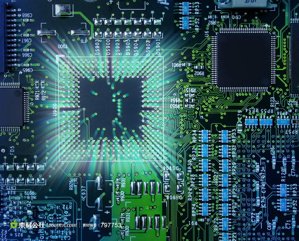


Just upload Gerber files, BOM files and design files, and the KINGFORD team will provide a complete quotation within 24h.