
Professional PCB manufacturing and assembly
Building 6, Zone 3, Yuekang Road,Bao'an District, Shenzhen, China
+86-13410863085Mon.-Sat.08:00-20:00

![What does PCBA mean [Professional introduction]](https://www.kingfordpcb.com/uploadfile/ueditor/image/202211/16675481160c8ff3.jpg)
What does PCBA mean [Professional introduction]
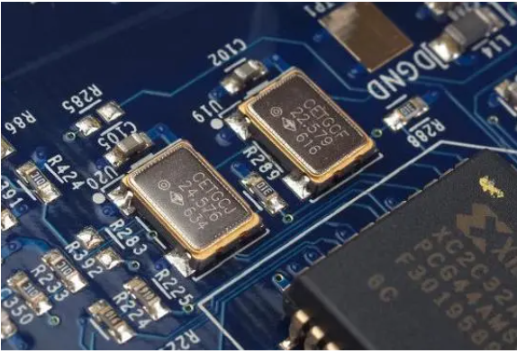
PCBA is the abbreviation of Printed Circuit Board+Assembly in English. In short, PCBA can be a series of technological processes consisting of SMT chip processing, DIP plug-in processing and PCBA testing.
1、 Code for Design and Inspection of PCBA Components
Inspection preparation The inspector must wear anti-static gloves and wrist watch, prepare calipers, electrical performance parameter instruments and other tools;
1. Technical requirements
1.1 PCBA component plates must be made of materials with a flame-retardant grade of 94-V0 or above, and have corresponding UL yellow cards;
1.2 The appearance of PCBA component plate shall be free of rough burrs, poor cutting, delamination and cracking;
1.3 The size, hole diameter and edge distance of PCBA assembly plate shall meet the requirements of the engineering drawing, and the unspecified tolerance value shall be ± 0.1mm; Unless otherwise required, the plate thickness is 1.6 ± 0.1mm;
1.4 PCBA components must be printed with production (design) date, UL symbol, certificate number, 94V-0 characters, factory logo and product model; If PCBA assembly is composed of multiple PCB boards, other PCB boards shall also be printed with the above contents;
1.5 The printing symbols and font size shall be clear and legible;
1.6 If resistance capacitance step-down circuit is used for PCBA components, half wave rectification circuit must be used to improve the safety and stability of the circuit;
1.7 If switching power circuit is adopted for PCBA components, standby power consumption must be less than 0.5W;
1.8 When using PCBA for European products, the standby power consumption must be less than 1W. If the American version PCBA customer has special requirements, the standby power consumption shall comply with the technical requirements;
1.9 LED except for power lamp φ 5 Amber highlights astigmatism, and all green or all red φ 3 Bright astigmatism; 1.10 The specified live wire (ACL), neutral wire (ACN), relay common terminal wire (ACL1), high or continuous wire (HI), low wire LO of PCBA components;
1.11 The welding fuse and CBB capacitor (resistance capacitance circuit) of PCBA components must be on the live wire (ACL);
1.12 ACL1 shall be connected to the live wire, HI or LO shall be connected to each end of the heater, and the common end of the heater shall be connected to the neutral wire;
1.13 The solder joints of PCBA components shall be free of faulty welding, continuous welding and desoldering, and the solder joints shall be smooth, uniform and free of bubbles, pinholes, etc;
2.jpg
2. Selection of components
2.1 Famous brand manufacturers are preferred for PCBA components, followed by manufacturers meeting international standards or industry standards; Components from manufacturers that do not adopt enterprise standards;
2.2 Integrated block components (IC) shall be industrial grade IC;
2.3 Connecting connectors and terminals must be UL certified and provided with certificates;
2.4 The metal film resistor with clear color ring shall be selected as the resistance components, and the manufacturer shall comply with the industry standard;
2.5 Electrolytic capacitor components shall be explosion-proof capacitors with working temperature of - 40-105 ℃, and the manufacturer shall comply with the industry standard;
2.6 Crystal components are selected as crystal components, RC or chip built-in is not recommended, and the manufacturer complies with international standards;
2.7 The diode or triode shall be selected from domestic well-known brands, which shall meet the industry standards;
2.8 The dumping switch shall be infrared photoelectric type instead of mechanical type;
2.9 The surface of the designated components must be printed with UL/VDE/CQC/symbols, trademarks, parameters and other contents clearly visible;
2.10 Relevant wire rods must have UL/VDE symbol, wire gauge, certification number, manufacturer name and other contents and be clearly visible;
3. Test and inspection
3.1 The PCBA components shall be installed on the corresponding test tooling platform, and the applicable parameters such as voltage and frequency shall be adjusted;
3.2 Whether the self inspection function of PCBA components meets the requirements of the functional specification, whether the relay output has abnormal sound, and whether the LED is fully lit evenly; 3.3 Whether the placement of PCBA component dumping device and the output function during dumping comply with the functional specification;
3.4 When the temperature probe of PCBA assembly is disconnected and short circuited, whether the output function and fault indication comply with the functional specification;
3.5 Whether the key function output of PCBA assembly meets the requirements of the functional specification;
3.6 Whether the ambient temperature indicator LED or the temperature displayed by the digital tube of the PCBA components meet the functional specifications;
3.7 Whether the power status indicator LED of PCBA assembly conforms to the functional specification;
3.8 Whether the intelligent control operation mode of PCBA components meets the functional specifications;
3.9 Whether the continuous operation mode of PCBA components meets the functional specifications;
3.10 Whether the standby power consumption of PCBA components meets the functional specifications;
3.11 When the voltage is adjusted to 80% of the rated voltage, whether the relay output has abnormal noise and whether the LED brightness is uniform;
3.12 If the voltage is adjusted to 1.24 times of the rated voltage, whether the relay output has abnormal noise and whether the LED brightness is uniform;
2、 PCBA General Appearance Inspection Specification
1. The wetting angle between the fillet weld with poor contact angle of the welding spot and the graphic end joint of the pad is greater than 90 °.
2. Upright: one end of the component leaves the bonding pad and is inclined or upright.
3. Short circuit: solders between two or more solder joints that should not be connected are connected, or solder joints are connected with adjacent wires.
4. Empty soldering: that is, the component lead and PCB solder joints are not connected by soldering tin.
5. False soldering: the component lead and PCB solder joint appear to be connected, but they are not actually connected.
6. Cold welding: solder paste at the solder joint is not completely melted or metal alloy is not formed.
7. Less tin (insufficient tin): the tin area or height between the component end and the PAD does not meet the requirements.
8. Too much tin (too much tin): the tin area or height between the component end and the PAD exceeds the requirements.
9. Blackening of solder joints: the solder joints are blackened and have no luster.
10. Oxidation: chemical reaction has occurred on the surface of components, circuits, PADs or solder joints and there are colored oxides.
11. Displacement: the component deviates from the predetermined position in the horizontal (horizontal), vertical (vertical) or rotation direction in the plane of the pad (based on the centerline of the component and the centerline of the pad).
12. Reverse polarity (reverse direction): reverse polarity of polar components or polarity inconsistent with the requirements of documents (BOM, ECN, component location map, etc.).
13. Floating height: there is a gap or height between components and PCB.
14. Wrong parts: the specification, model, parameter, shape and other requirements of components are inconsistent with (BOM, samples, customer data, etc.).
15. Tin tip: the solder joints of components are not smooth, and the solder tips are stored.
16. Multiple parts: According to BOM, ECN or template, the parts that should not be pasted or have redundant parts on PCB are multiple parts.
17. Missing parts: According to BOM, ECN or sample plate, the parts that should be mounted on the position or PCB but not on the PCB are short.
18. Misalignment: the position of components or component pins is moved to the position of other PADs or pins.
19. Open circuit (open circuit): PCB circuit is disconnected.
20. Side placing (side standing): Side placing of pieces with different width and height.
21. Inverted (reversed): the two opposite sides of the component are interchangeable (such as the side with silk screen mark and the side without silk screen mark are upside down), and sheet resistance is common.
22. Tin bead: small tin point between component pins or outside PAD.
23. Bubbles: There are bubbles in solder joints, components or PCBs.
24. Tin loading (tin climbing): the tin eating height of component solder joints exceeds the required height.
25. Tin crack: the solder joint is cracked.
26. Hole plug: PCB plug-in hole or through hole is blocked by soldering or other means.
27. Damage: crack, cutting or damage of components, plate bottom, plate surface, copper foil, circuit, through-hole, etc.
28. Blurred screen printing: the text or screen printing of components or PCBs is blurry or broken, and cannot be identified or blurry.
29. Dirt: the board surface is unclean, with foreign matters or stains.
30. Scratch: PCB or key scratch and bare copper foil.
31. Deformation: components or PCB body or corners are not on the same plane or bent.
32. Foaming (delamination) PCB or components are delaminated with copper and platinum with gaps.
33. Excess glue (too much glue) (too much red glue) or overflow the required range.
34. Little glue (too little red glue) or not reaching the required range.
35. Pinhole (concave point): PCB, PAD, solder joint, etc. have pinhole concave points.
36. Burr (peak): PCB edge or burr exceeds the required range or length.
37. Gold finger impurities: there are pits, tin spots or anti soldering oil on the surface of gold finger coating.
38. Gold finger scratch: the gold finger coating surface has scratch marks or bare copper platinum.


Just upload Gerber files, BOM files and design files, and the KINGFORD team will provide a complete quotation within 24h.