
Professional PCB manufacturing and assembly
Building 6, Zone 3, Yuekang Road,Bao'an District, Shenzhen, China
+86-13410863085Mon.-Sat.08:00-20:00

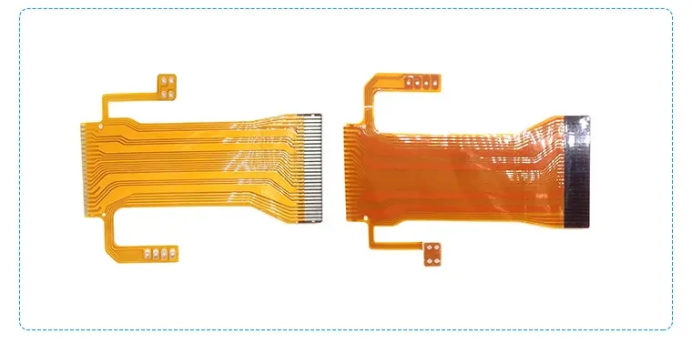
Progress in full print fabrication of multilayer embedded flexible circuits
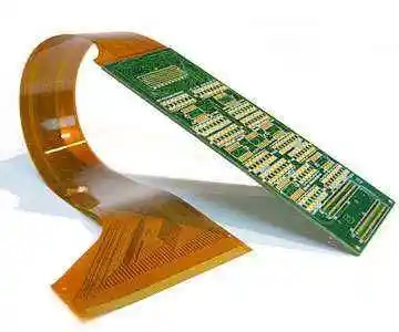
Flexible printed circuits are expected to replace traditional electronic devices based on photolithography due to their advantages of environmental protection, low cost, and easy flexibility. Ink jet printing technology can directly realize the patterning of metal nanoparticles, which is one of the most promising methods to prepare nano printed electronic devices. However, the application of ink-jet printing technology in the field of high-precision and high integration circuit preparation is limited due to the difficulties of ink droplet spreading and merging.
With the strong support of the National Natural Science Foundation of China, the Ministry of Science and Technology and the Chinese Academy of Sciences, the scientific researchers in the Key Laboratory of Green Printing of the Institute of Chemistry, Chinese Academy of Sciences deeply and systematically studied the interaction between printing ink droplets and substrate, and carried out a series of extensive and in-depth research in the field of controllable high-precision printing and printing technology by regulating the wetting behavior of ink droplets on the substrate surface (Adv. Mater. 2014, 26, 6950-6958). They successfully prepared a series of high-precision patterns by adjusting the characteristics of materials such as ink and substrate: the line width can reach 5% by using the "coffee ring" phenomenon μ M of metal nanoparticles (Adv. Mater. 2013, 25, 6714-6718); Printing and preparing high-precision three-dimensional functional patterns by using three-phase line slip phenomenon of printing ink drops (Adv. Opt. Mater. 2014, 2, 34-38; Adv. Funct. Mater. 2015, 25, 2237-2242); A series of special three-dimensional cylindrical structures with controllable shape were prepared by magnetic field induced dynamic retraction of three-phase lines (Small 2015, 11, 1900-1904); High precision micro pits and groove structures were prepared using soft substrate "ink-jet imprinting" (Adv. Funct. Mater. 2015, 25, 3286-3294); The conductive pattern with an accuracy of 30 nm was prepared by controlling the assembly and printing of nano materials on the printed electrode template (Adv. Mater. 2015, 273928-3933). They used these printed and printed functional patterns to achieve plasma light wave transmission (Adv. Mater. 2014, 26, 2501-2507), highly sensitive detection (Angelw. Chem. Int. Ed. 2014, 53, 5791-5795; Nanoscale 2015, 7, 421-425), quantum dot pattern (Small 2015, 11, 1649-1654), biological cell separation (ACS Appl. Mat. Interfaces 2015, 7, 9060-9065) Applications such as microfluidic channel (Lab on a Chip 2015, 71759-64) and high-precision flexible circuit preparation (Adv. Mater. 2015, 273928-3933).
On the basis of the above research, they realized the direct preparation of high-precision embedded conductive silver wire by printing conductive ink containing nano particles on the polymerizable liquid substrate and ingeniously utilizing the dynamic wrapping effect of the liquid substrate on the printing ink droplets. Due to the influence of viscosity and surface tension of conductive ink for ink-jet printing, it is very challenging to realize its integration into a line in another liquid. They solved this problem by regulating the rheological behavior of the liquid substrate and the properties of the nano silver conductive ink, realizing the controllable wrapping of ink droplets by the liquid substrate, and effectively inhibiting the diffusion of ink droplets and the "coffee ring" effect (Figure 1). Based on this, the orifice diameter is 25 μ The common commercial printer of m has prepared a line width of about 1-2 μ M conductive silver wire, about 20 times higher than the usual ink-jet printing accuracy. The fabricated high-precision circuit is directly embedded in the substrate, avoiding the subsequent packaging steps. Electrical tests show that the embedded micro cable prepared by this method has excellent conductivity. They further used this "liquid film embedded printing" to directly print the multilayer circuit layer by layer, reaching 60 μ M The integration degree of three layers of circuits embedded in transparent films.
The "liquid film embedded printing" in this work is a universal method, which is also applicable to carbon nanotubes, graphene and other conductive materials. It is of great significance to improve the accuracy and integration of printing circuits, and to prepare ultrahigh transparent embedded electronic devices. It also lays a technical foundation for printing and preparing highly integrated and high-precision three-dimensional structure circuits.
The circuit board manufacturers and circuit board designers will explain the progress made in full print preparation of multilayer embedded flexible circuits.


Just upload Gerber files, BOM files and design files, and the KINGFORD team will provide a complete quotation within 24h.