
Professional PCB manufacturing and assembly
Building 6, Zone 3, Yuekang Road,Bao'an District, Shenzhen, China
+86-13410863085Mon.-Sat.08:00-20:00

PCB Technology Waste PCB Treatment and Reuse Technology
Recycling of waste circuit boards is a new industry. With the scrapping of a large number of household appliances, the number of waste circuit boards is growing, and its recycling value has also attracted many investors' attention, becoming a promising industry. The composition of waste circuit boards is complex, and it is difficult to recycle them. In addition, a large amount of organic substances are added to the circuit boards during the production process. A little carelessness in the recycling process of waste circuit boards may cause serious pollution to the environment. At present, the recovery and treatment technology of waste PCB in China is still relatively backward, and the development of advanced waste PCB treatment technology has become the object of research by many technicians. In this paper, the current waste PCB recycling technology is introduced and evaluated.
1、 Composition of waste circuit board
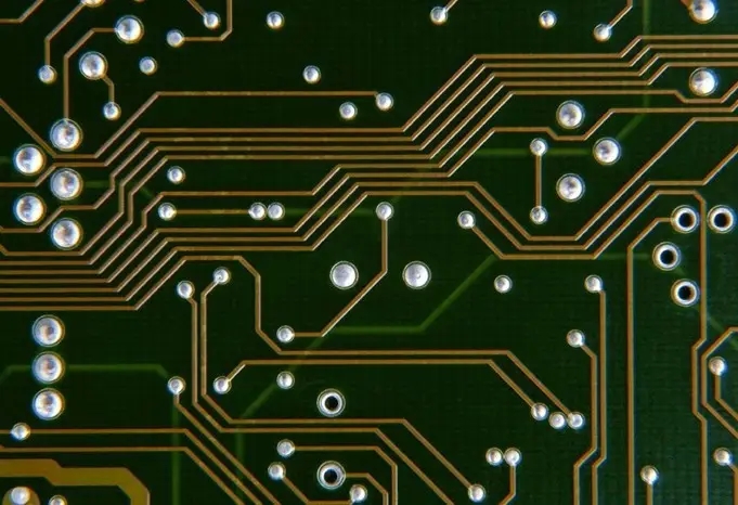
Waste circuit boards include waste copper clad laminate (CCL), waste printed circuit boards (PCBs), and printed circuit board cards with integrated circuits and electronic devices (generally referred to as waste circuit boards).
1. Waste copper clad plate
Copper clad laminate is the raw material for the production of printed circuit boards, which is mainly composed of substrate, copper foil and adhesive. The main materials of the base plate are synthetic resin and reinforcement materials, of which the synthetic resin mainly includes phenolic resin, epoxy resin, polytetrafluoroethylene, etc. The reinforcement materials generally include paper and cloth.
The surface of the substrate is copper foil, which is produced by mechanical processing and electrowinning. At present, electrowinning is the main production method, and the thickness of copper foil is generally 18 μ m、25 μ m、35 μ m、70 μ m. And 105 μ m。 Copper foil is firmly adhered to the substrate with adhesive to form a copper clad plate.
At present, a large number of copper clad laminates are used in China, including phenolic paper clad laminates, epoxy paper clad laminates, epoxy glass cloth clad laminates, polytetrafluoroethylene clad laminates, and polyimide flexible copper clad laminates. Among them, epoxy (paper or glass cloth) copper-clad laminates are used for civil appliances, instruments and meters above the middle grade, with a large amount. Phenolic paper copper clad laminate is widely used for medium and low grade civil electrical appliances.
Scrap copper clad laminate is the defective products and leftovers produced in the production process. It is generally called yellow plate because of the pressed copper foil on the surface. The copper content of waste copper clad laminate varies from about 15% to more than 70%, which is an important resource for copper recovery.
2. Waste printed circuit board
Printed circuit board is called PCB for short. Generally, the conductive graphics designed on the insulating material as per the predetermined design into printed circuit, printed original or combination of both are called printed circuit, and the conductive graphics that provide electrical connection between components on the insulating substrate are called printed circuit. Printed circuit or finished board of printed circuit is called printed circuit board.
The printed circuit board is mainly used to provide support for the fixed assembly of various electronic components such as integrated circuits, realize the wiring and electrical connection or electrical insulation between various electronic components such as integrated circuits, provide solder resistance graphics for automatic soldering, and provide identification characters and graphics for component insertion, inspection and maintenance.
Almost all the electronic devices we can see have PCB, such as calculators, computers, communication electronic devices, military weapon systems, etc. As long as there are integrated circuits and other electronic components, the electrical interconnection between them should use PCB. Common computer boards are basically epoxy glass cloth based double-sided printed circuit boards. One side is a plug-in component, and the other side is a component leg welding surface. The welding points are generally very regular.
The defective products produced in the production process of printed circuit boards are often referred to as waste printed circuit boards. Because they are mainly green, they are also called green boards. When making PCB, although some copper has been corroded and the copper content of PCB is lower than that of CCL, PCB is still one of the resources of copper recovery.
3. Waste circuit board
Waste circuit boards mainly come from various discarded electrical appliances. There are many kinds of waste circuit boards, such as green boards and yellow boards. The green boards are mainly disassembled from waste TV sets, computers and communication equipment, which are of high value; The yellow board is mainly disassembled from tape recorders, audio equipment, washing machines, and air conditioners, with low value.
The components of waste circuit boards are relatively complex. In addition to printed circuit boards, they also contain integrated circuits and various electronic components. The main components are silicon dioxide, copper foil, lead, tin, iron trace precious metals, plastics, resins, paints and other organic substances. Therefore, the treatment is more difficult than that of waste copper clad boards and waste printed circuit boards.
2、 Treatment of Waste Circuit Board by Gravity Beneficiation Technology
This technology is based on the principle of gravity beneficiation. First, the waste board is crushed to a certain particle size, and then it is treated with a shaking table using water as the medium. Finally, the purpose of separating copper from glass fiber and other reinforcement materials is achieved. The shaking table is a inclined bed surface with many parallel multiple strips or grooves in the longitudinal direction. When working, it makes asymmetric reciprocating motion with the help of mechanical power. At the same time, it works in combination with the thin inclined plane water flow to make the particles loose, layered and zoned on the bed surface, and enable minerals to be sorted according to different densities. The final product of waste CCL treated by gravity beneficiation is copper powder, which is strictly a copper scrap with a diameter of about 20~40 mesh. Since the shaker is a kind of beneficiation equipment, the final product in the beneficiation process is concentrate, not pure metal, so the copper powder obtained by treating waste circuit boards with this method contains about 85%~95% copper. If the circuit board without integrated circuits and components is processed, the copper powder contains a small amount of iron, lead and tin.
The raw materials are first roughly crushed by the crusher, and then enter the second crushing process, so that they become crushed materials with a particle size of about 20~40. During the crushing process, water is continuously added, which not only plays a role in cooling equipment, but also makes the crushed materials and water form a slurry, which not only avoids dust pollution in the crushing process, but also facilitates the direct flow of crushed materials into the next process. The slurry formed after crushing enters the shaking table for gravity separation. Under the action of vibration and gravity, the copper particles and broken glass fibers are separated. The copper particles slip into a special collection tank and are regularly taken out of the water. They are dried by a dryer and then dried to obtain the final product copper powder. In order to improve the recovery rate, the materials passing through the first shaker shall pass through the second shaker to further recover the copper. The copper powder obtained by the first shaker is of good quality, with copper content between 85% and 95%. The copper powder obtained by the second shaker is of high impurities, generally with copper content below 80%. After the separation of copper powder, the cullet fiber slurry enters the multistage sedimentation tank for natural sedimentation, and the water is recycled.
After years of practice, it has been proved that the gravity beneficiation technology has the best effect on the treatment of waste CCL, followed by the treatment of printed circuit boards, but it can not deal with waste circuit boards. At present, before disposing of waste circuit boards, some enterprises often manually remove the tin in a simple tin removal furnace, and then crush the electronic components. With the continuous development of electronic industry technology, the yield of copper clad laminate and the qualification rate of printed circuit board are constantly improving, and the amount of waste copper clad laminate is gradually decreasing. At the same time, due to the increase of discarded mechanical and electrical products, the number of waste circuit boards is also increasing rapidly. In the future, the waste circuit boards will be the ones that will be handled more.
Using gravity beneficiation technology to treat waste circuit boards has the advantages of less investment and simple process, but it can not directly treat waste circuit boards. The copper powder produced by this technology contains high impurities, which is not convenient for direct utilization. Moreover, the copper contains lead and tin, and the metal recovery rate is low. In addition, the resulting glass fiber scrap is difficult to handle and will have an impact on the environment during the stacking process. At present, some enterprises try to make them into building materials such as bricks or other materials, but these materials made of organic adhesives have a short service life. Once damaged, they will become a source of pollution again.
3、 Pyro smelting technology
Pyro smelting technology mainly includes blast furnace smelting and Kaldor furnace smelting. The advantage of pyrometallurgical treatment of waste circuit board is that the glass fiber in the waste circuit board is fully used to make it play the role of flux in the smelting process, and form stable silicate slag with impurities and other fluxes in the smelting process, which solves the problem of passive treatment of glass fiber debris by wet treatment.
1. Blast furnace smelting technology
Blast furnace smelting technology is mainly used to smelt low-grade waste copper, which is one of the traditional three-stage method, and is also the main method to treat waste circuit boards in China at present. The method can simultaneously treat waste copper clad laminate, waste printed circuit board and waste circuit board. The waste circuit board is directly added into the blast furnace, coke is used as raw material, and limestone (or lime) and other fluxes are added, in which iron and calcium are directly slagged with silica to form molten slag. Copper is recovered in the reducing atmosphere, and finally coarse copper ingots are formed.
The waste circuit board contains a small amount of precious metals, mainly gold and silver. Copper is a good collector for gold and silver. Therefore, precious metals are melted in copper melt and enter the hearth during smelting. The circuit board card contains lead and tin alloy solder. In the reducing atmosphere, most tin can be well dissolved in copper, while some lead enters the hearth and the other enters the slag. The final product of blast furnace is crude copper ingot, with copper content generally between 80% and 90%, containing trace precious metals. Copper ingots are used as furnace charge by copper smelting enterprises to further recover copper and precious metals.
The main component of the glass fiber in the waste circuit board is silicon oxide, which acts as a flux in the smelting process, so silicon oxide solvent can be reduced or basically not added. In the smelting process, glass fiber and other impurities form silicate slag. The main components of the molten blast furnace slag are silicate (calcium silicate and ferrous silicate). After water quenching treatment in front of the furnace, water quenched slag with a diameter of about 5-10mm is formed. The water quenched slag has stable composition, and can be directly used as raw material for cement production, or as sandblasting for rust removal in shipbuilding industry. It not only eliminates the problem of debris pollution caused by other methods, but also improves the utilization value of waste glass fiber.
At present, the main problem of waste PCB treatment in blast furnace is environmental problem. Waste circuit boards contain a large amount of organic substances, which will produce dioxins during combustion and have an impact on the environment. The formation temperature of dioxins is about 400 ℃ - 800 ℃. When the temperature is higher than 800 ℃, dioxins will decompose, but when the flue gas slowly cools down, there is a possibility of re synthesis. Therefore, a good environmental protection treatment system must be established.
2. Waste circuit board treated by Kaldor furnace
The progressiveness of the Kaldor furnace in treating waste circuit boards is mainly reflected in the high metal recovery rate and good environmental benefits. Waste circuit boards can be directly added to the Kaldor furnace as furnace materials without any treatment. The Kaldor furnace with oxygen top blowing uses oil or natural gas as the fuel, which has high thermal efficiency. At the same time, the energy consumption is greatly reduced by using the heat generated by the burning of organic materials. The generated flue gas does not spill and can be well collected. It is also equipped with a perfect environmental protection system to cool the high-temperature flue gas to below 400 ℃ in an instant, eliminating dioxin pollution. In order to solve the odor of flue gas from waste PCB combustion, the environmental protection system is equipped with activated carbon adsorption facilities to eliminate the odor of flue gas.
The Kaldor furnace is operated intermittently, and the copper content of raw materials can be high or low, which is very suitable for the treatment of waste circuit boards, especially for the circuit boards with electronic components. It eliminates the process of manual removal of electronic components. In the smelting process, gold, silver and other precious metals are all melted in copper, which improves the recovery rate of precious metals. The final product of Kaldor furnace is crude copper, which needs further refining to obtain refined copper. Kaldor furnace has many advantages, but due to large investment and high equipment depreciation cost, it is only suitable for large-scale treatment of electronic waste, and it is difficult to apply it to electronic waste treatment in China.
4、 Disposal of waste circuit board by incineration and smelting process
The pollutants to the environment during the smelting process of waste circuit boards mainly come from the combustion of organic substances. Therefore, the focus of this technology is to pretreat the waste circuit boards before they are put into the furnace, burn off the organic substances, and effectively treat the flue gas to eliminate their pollution to the environment, and then smelt the burned materials.
Some copper smelting enterprises in Japan have adopted incineration smelting technology to treat waste PCB, and achieved good results. First, the waste circuit board is incinerated in a specially made incinerator at a temperature of about 800 ℃ to ensure that copper, precious metals and glass fibers do not melt during the incineration process, so as to fully burn organics. The flue gas generated by combustion enters the secondary combustion chamber and continues to burn at 1200 ℃ to decompose dioxin. The flue gas passing through the secondary combustion chamber quickly enters the rapid cooling facility, reducing the flue gas temperature to below 400 ℃ in a few seconds, avoiding the re synthesis of dioxins and eliminating pollution.
The waste circuit board after incineration has no problem of organic pollution. The simplest treatment method is to use it as the raw material of regenerated copper, which can be added into the anode furnace as the ingredient. Valuable metals can be effectively recovered through processes such as smelting in the anode furnace, electrolysis, and precious metal recovery from anode slime. The recovery rate of copper and precious metals reaches more than 98%, which is a good technology for processing circuit boards at present.
In the smelting process of regenerated copper, slagging agent silicon dioxide needs to be added. The main impurity glass fiber in the waste circuit board, namely silicon dioxide, can replace some solvents. After slagging, the flux and impurities form silicate, which is a good additive for cement production and a rust remover (sand blasting) for shipbuilding industry. In the incineration process, the thermal energy is mainly the burning of organic substances in waste circuit boards, which can greatly reduce energy consumption and achieve the effect of energy conservation. A small amount of diesel oil shall be added as fuel at the beginning of incineration and when the temperature is low.
Incineration smelting process has become a classic process for Japanese copper recycling enterprises to treat waste PCB. At present, there are two kinds of incinerators, one is fixed incinerator, the other is rotary incinerator. The basic principles of both incinerators are the same.
5、 Other methods
At present, some units are studying the technology of treating waste copper clad laminates by retorting, so that the waste copper clad laminates can be retorted at high temperatures, in which the epoxy resin volatilizes at high temperatures and is recycled in the condenser. There is no organic matter in the waste circuit board after retorting. After smelting, crude copper is obtained. The crude copper is further refined in the anode furnace and electrolysis, and precious metals are recovered from the electrolytic anode slime. The advantage of this method is that the epoxy resin is recovered, which not only avoids the pollution problem caused by organic burning, but also comprehensively recovers the epoxy resin. This technology is currently in the experimental stage.
The circuit board is the basic material of electronic appliances. China has become a large country in the production of circuit boards. In the production and manufacturing of copper clad boards and printed circuit boards, the number of defective products and leftovers has increased year by year. At the same time, as China's household appliances have entered the peak of scrapping, the number of waste circuit boards is increasing rapidly. Therefore, the research and development of harmless disposal of waste PCB technology has become a major topic in the field of renewable resources.


Just upload Gerber files, BOM files and design files, and the KINGFORD team will provide a complete quotation within 24h.